- 您現(xiàn)在的位置:買賣IC網(wǎng) > PDF目錄358881 > LMH6739MQ (NATIONAL SEMICONDUCTOR CORP) Very Wideband, Low Distortion Triple Video Buffer PDF資料下載
參數(shù)資料
| 型號: | LMH6739MQ |
| 廠商: | NATIONAL SEMICONDUCTOR CORP |
| 元件分類: | 音頻/視頻放大 |
| 英文描述: | Very Wideband, Low Distortion Triple Video Buffer |
| 中文描述: | 1 CHANNEL, VIDEO AMPLIFIER, PDSO16 |
| 封裝: | SSOP-16 |
| 文件頁數(shù): | 3/10頁 |
| 文件大?。?/td> | 796K |
| 代理商: | LMH6739MQ |
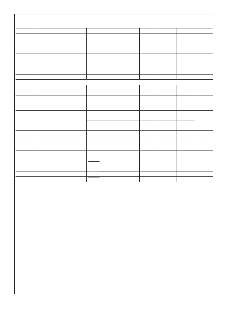
Electrical Characteristics
(Note 2) (Continued)
A
V
= +2, V
CC
=
±
5V, R
L
= 100
; unless otherwise specified.
Symbol
Parameter
CMRR
Common Mode Rejection Ratio
(Note 6)
I
CC
Supply Current (Note 6)
Conditions
Min
46
44
Typ
50
Max
Units
dB
All three amps Enabled, No
Load
R
L
=
∞
R
L
=
∞
32
35
40
2.2
1.3
525
mA
Supply Current Disabled V
+
Supply Current Disabled V
Internal Feedback & Gain Set
Resistor Value
Gain Error
Miscellaneous Performance
R
IN
+
Non-Inverting Input Resistance
C
IN
+
Non-Inverting Input Capacitance
R
IN
Inverting Input Impedance
1.9
1.1
450
mA
mA
375
R
L
=
∞
0.2
±
1.1
%
1000
.8
30
k
pF
Output impedance of input
buffer.
DC
R
L
= 100
R
O
V
O
Output Impedance
Output Voltage Range (Note 6)
0.05
±
3.5
±
3.25
±
3.1
±
3.65
±
3.5
±
1.9
±
1.7
80
60
V
R
L
=
∞
±
3.8
CMIR
Common Mode Input Range
(Note 6)
Linear Output Current (Note 3)
(Note 6)
Short Circuit Current (Note 5)
CMRR
>
40 dB
±
2.0
V
I
O
V
IN
= 0V, V
OUT
<
±
30 mV
90
mA
I
SC
V
IN
= 2V Output Shorted to
Ground
Disable Pin = V
+
Disable Pin = 0V
Disable Pin
≤
V
DMAX
Disable Pin
≥
V
DMIN
160
mA
I
IH
I
IL
V
DMAX
V
DMIM
Disable Pin Bias Current High
Disable Pin Bias Current Low
Voltage for Disable
Voltage for Enable
10
μA
μA
V
V
350
0.8
2.0
Note 1:
Absolute Maximum Ratings indicate limits beyond which damage to the device may occur. Operating Ratings indicate conditions for which the device is
intended to be functional, but specific performance is not guaranteed. For guaranteed specifications, see the Electrical Characteristics tables.
Note 2:
Electrical Table values apply only for factory testing conditions at the temperature indicated. Factory testing conditions result in very limited self-heating of
the device such that T
J
= T
A
. No guarantee of parametric performance is indicated in the electrical tables under conditions of internal self heating where T
J
>
T
A
.
See Applications Section for information on temperature de-rating of this device. Min/Max ratings are based on product characterization and simulation. Individual
parameters are tested as noted.
Note 3:
The maximum output current (I
OUT
) is determined by device power dissipation limitations. See the Power Dissipation section of the Application Section for
more details.
Note 4:
Human body model: 1.5 k
in series with 100 pF. Machine model: 0
in series with 200 pF.
Note 5:
Short circuit current should be limited in duration to no more than 10 seconds. See the Power Dissipation section of theApplication Section for more details.
Note 6:
Parameter 100% production tested at 25 C.
L
www.national.com
3
相關PDF資料 |
PDF描述 |
|---|---|
| LMH6739MQX | Very Wideband, Low Distortion Triple Video Buffer |
| LMK316BJ475KL | UNREGULATED 60-mA CHARGE PUMP VOLTAGE INVERTER |
| LMK316BJ475ML | Low Drop Output Voltage Regulator |
| LMK83S018H2 | LMM83S018C2N |
| LML337HVH | 3-Terminal Adjustable Negative Regulators (High Voltage) |
相關代理商/技術參數(shù) |
參數(shù)描述 |
|---|---|
| LMH6739MQ/NOPB | 功能描述:緩沖器和線路驅(qū)動器 RoHS:否 制造商:Micrel 輸入線路數(shù)量:1 輸出線路數(shù)量:2 極性:Non-Inverting 電源電壓-最大:+/- 5.5 V 電源電壓-最小:+/- 2.37 V 最大工作溫度:+ 85 C 安裝風格:SMD/SMT 封裝 / 箱體:MSOP-8 封裝:Reel |
| LMH6739MQ/NOPB | 制造商:Texas Instruments 功能描述:Buffer IC |
| LMH6739MQX | 功能描述:緩沖器和線路驅(qū)動器 RoHS:否 制造商:Micrel 輸入線路數(shù)量:1 輸出線路數(shù)量:2 極性:Non-Inverting 電源電壓-最大:+/- 5.5 V 電源電壓-最小:+/- 2.37 V 最大工作溫度:+ 85 C 安裝風格:SMD/SMT 封裝 / 箱體:MSOP-8 封裝:Reel |
| LMH6739MQX/NOPB | 功能描述:緩沖器和線路驅(qū)動器 RoHS:否 制造商:Micrel 輸入線路數(shù)量:1 輸出線路數(shù)量:2 極性:Non-Inverting 電源電壓-最大:+/- 5.5 V 電源電壓-最小:+/- 2.37 V 最大工作溫度:+ 85 C 安裝風格:SMD/SMT 封裝 / 箱體:MSOP-8 封裝:Reel |
| LMH681MA/NOPB | 制造商:Texas Instruments 功能描述: |
發(fā)布緊急采購,3分鐘左右您將得到回復。