- 您現(xiàn)在的位置:買賣IC網(wǎng) > PDF目錄358881 > LMH6678LQX (NATIONAL SEMICONDUCTOR CORP) Low Power 2-Channel Central-Office xDSL Driver PDF資料下載
參數(shù)資料
| 型號(hào): | LMH6678LQX |
| 廠商: | NATIONAL SEMICONDUCTOR CORP |
| 元件分類: | 通用總線功能 |
| 英文描述: | Low Power 2-Channel Central-Office xDSL Driver |
| 中文描述: | DUAL LINE DRIVER, QCC24 |
| 封裝: | 5 X 4 MM, LLP-24 |
| 文件頁(yè)數(shù): | 14/17頁(yè) |
| 文件大?。?/td> | 1792K |
| 代理商: | LMH6678LQX |
第1頁(yè)第2頁(yè)第3頁(yè)第4頁(yè)第5頁(yè)第6頁(yè)第7頁(yè)第8頁(yè)第9頁(yè)第10頁(yè)第11頁(yè)第12頁(yè)第13頁(yè)當(dāng)前第14頁(yè)第15頁(yè)第16頁(yè)第17頁(yè)

Application Notes
(Continued)
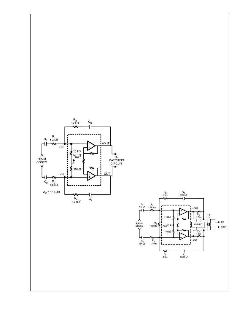
If additional gain is required, the gain can be increased with
positive feedback using the circuit of
Figure 6
. In this case
the voltage gain A
V
will be
A
V
=5.4*(1-K)/(1-5.4*K)
Where
K = (R
1
||10K)/(R
||10K + R
2
) = 10K*R
1
(10K*R
1
+ R
1
R
2
+
10K*R
2
) and R
1
= R
3
, R
2
= R
4
It is suggested to choose R
<
3K so that the 15% tolerance
of the input resistance will not greatly affect the gain. Fur-
thermore, this circuit will have a differential input resistance
of
R
IN_DIFF
= 2*R
1
2 *R
2
/(4.4)
which may be negative in band. Usually no stability problems
are seen if this |R
| is chosen larger than 500
. To minimize
distortion caused by loading on the Codec outputs, |R
| is
usually chosen to be 1k
or more. Additional blocking ca-
pacitors C
and C
must be inserted in series with R
and R
4
to prevent the circuit from latching. C
and C
should be
chosen to be less than 1/5 of C
1
to avoid large signal
oscillation.
ACTIVE TERMINATION CIRCUIT
The LMH6678 can be used to synthesize the output imped-
ance by using positive feedback to increase the output re-
sistance. In ADSL this technique is often used to lower the
total power consumption of the line driver by reducing the
voltage across the series termination resistors. This ap-
proach gives slightly higher power consumption but better
return loss in the downstream band compared to the R-C
termination of Figure 5. The equations that follow and Figure
7 describe how to implement this technique with the
LMH6678.
1.
Pick positive feedback factor (also called the resistance
gain), A
Z
.
2.
Pick desired output resistance, R
OUT
, seen by the line.
3.
Calculate transformer turns ratio based on A
, line driver
voltage swing, and transformer insertion loss (TIL). R
L
is
the line impedance, 100
for ADSL.
N = [(V
LINEPP
/(2 * 11.2)]* [(1 + R
OUT
/( R
L
* A
Z
)] * 10
(TIL/20)
4.
Calculate R
4
from R
OUT
, A
Z
, and N
R
4
= R
OUT
/ (2 * A
Z
* N
2
)
5.
Calculate the resistance looking into the transformer
secondary (chip side).
R
SEC
= R
L
/ N
2
6.
Calculate K
1
.
K
1
= (A
Z
- 1)/(5.4 * A
Z
)
7.
Calculate K
2
.
K
2
= R
SEC
/( R
SEC
+ 2 * R
4
)
8.
Pick a value for R
2
. Typically 3k
is a good value.
9.
Calculate R
EQ
.
R
EQ
= R
2
/(1-5.4* K
2
)
(Note R
EQ
is usually negative.)
10. Calculate R
IN
R
IN
= [(K
1
*R
2
)/(1-K
1
)*10k]/[10k-(K
1
*R
2
)/(1-K
1
)]
11. Calculate the gain without the input voltage divider.
A
V1
= N*5.4*K
2
* [(R
EQ
//10k)/(R
IN
+ R
EQ
//10k)] /(10
TIL/20
)
12. . Calculate A
VTOTAL
the final required gain from input to
the line.
A
VTOTAL
= V
LINERMS
/V
INRMS
13. . Calculate the voltage divider network of R1 and R3
using A
V1
, transformer insertion loss (TIL),
R
1
= R
IN
* [A
V1
/(A
VTOTAL
*10
TIL/20
)]
R
3
= (2 * R
IN
)/[1 - (A
VTOTAL
*10
TIL/20
)/ A
V1
]
The example shown in Figure 7 is designed to the following
parameters:
V
LINERMS
= 3.13V
(19.8 dBm output power)
A
Z
= 4.5
R
OUT
= 65
(13.5dB return loss)
Crest Factor = 5.8
@
nominal 12V supply
Transformer Insertion Loss = 0.4dB
V
INRMS
= 350mV
(AFE output level)
20084046
FIGURE 6. Increasing Gain
20084047
FIGURE 7. Active Termination Application
L
www.national.com
14
相關(guān)PDF資料 |
PDF描述 |
|---|---|
| LMH6678 | Low Power 2-Channel Central-Office xDSL Driver |
| LMH6704MA | 650 MHz Progammable Gain Buffer with Disable |
| LMH6704MAX | 650 MHz Progammable Gain Buffer with Disable |
| LMH6704MF | 650 MHz Progammable Gain Buffer with Disable |
| LMH6704MFX | 650 MHz Progammable Gain Buffer with Disable |
相關(guān)代理商/技術(shù)參數(shù) |
參數(shù)描述 |
|---|---|
| LMH6682 | 制造商:NSC 制造商全稱:National Semiconductor 功能描述:190MHz Single Supply, Dual and Triple Operational Amplifiers |
| LMH6682MA | 制造商:Texas Instruments 功能描述:OP Amp Dual Volt Fdbk ±6V/12V 8-Pin SOIC N Rail 制造商:Texas Instruments 功能描述:AMP, VIDEO DUAL, SMD, SOIC8, 6682 |
| LMH6682MA/NOPB | 功能描述:運(yùn)算放大器 - 運(yùn)放 RoHS:否 制造商:STMicroelectronics 通道數(shù)量:4 共模抑制比(最小值):63 dB 輸入補(bǔ)償電壓:1 mV 輸入偏流(最大值):10 pA 工作電源電壓:2.7 V to 5.5 V 安裝風(fēng)格:SMD/SMT 封裝 / 箱體:QFN-16 轉(zhuǎn)換速度:0.89 V/us 關(guān)閉:No 輸出電流:55 mA 最大工作溫度:+ 125 C 封裝:Reel |
| LMH6682MAX | 功能描述:運(yùn)算放大器 - 運(yùn)放 RoHS:否 制造商:STMicroelectronics 通道數(shù)量:4 共模抑制比(最小值):63 dB 輸入補(bǔ)償電壓:1 mV 輸入偏流(最大值):10 pA 工作電源電壓:2.7 V to 5.5 V 安裝風(fēng)格:SMD/SMT 封裝 / 箱體:QFN-16 轉(zhuǎn)換速度:0.89 V/us 關(guān)閉:No 輸出電流:55 mA 最大工作溫度:+ 125 C 封裝:Reel |
| LMH6682MAX/NOPB | 功能描述:運(yùn)算放大器 - 運(yùn)放 RoHS:否 制造商:STMicroelectronics 通道數(shù)量:4 共模抑制比(最小值):63 dB 輸入補(bǔ)償電壓:1 mV 輸入偏流(最大值):10 pA 工作電源電壓:2.7 V to 5.5 V 安裝風(fēng)格:SMD/SMT 封裝 / 箱體:QFN-16 轉(zhuǎn)換速度:0.89 V/us 關(guān)閉:No 輸出電流:55 mA 最大工作溫度:+ 125 C 封裝:Reel |
發(fā)布緊急采購(gòu),3分鐘左右您將得到回復(fù)。