- 您現(xiàn)在的位置:買賣IC網(wǎng) > PDF目錄30759 > LMH6643MDC (NATIONAL SEMICONDUCTOR CORP) 2 CHANNEL, VIDEO AMPLIFIER, UUC PDF資料下載
參數(shù)資料
| 型號: | LMH6643MDC |
| 廠商: | NATIONAL SEMICONDUCTOR CORP |
| 元件分類: | 音頻/視頻放大 |
| 英文描述: | 2 CHANNEL, VIDEO AMPLIFIER, UUC |
| 封裝: | DIE |
| 文件頁數(shù): | 9/26頁 |
| 文件大小: | 902K |
| 代理商: | LMH6643MDC |
第1頁第2頁第3頁第4頁第5頁第6頁第7頁第8頁當(dāng)前第9頁第10頁第11頁第12頁第13頁第14頁第15頁第16頁第17頁第18頁第19頁第20頁第21頁第22頁第23頁第24頁第25頁第26頁

Application Notes (Continued)
Single Supply, Low Power Photodiode Amplifier:
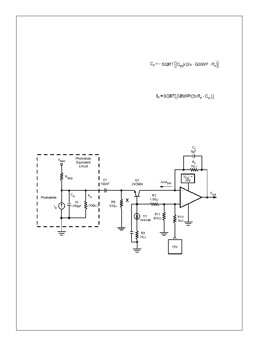
The circuit shown in
Figure 3 is used to amplify the current
from a photo-diode into a voltage output. In this circuit, the
emphasis is on achieving high bandwidth and the transim-
pedance gain setting is kept relatively low. Because of its
high slew rate limit and high speed, the LMH664X family
lends itself well to such an application.
This circuit achieves approximately 1V/mA of transimped-
ance gain and capable of handling up to 1mA
pp from the
photodiode. Q1, in a common base configuration, isolates
the high capacitance of the photodiode (C
d) from the Op
Amp input in order to maximize speed. Input is AC coupled
through C1 to ease biasing and allow single supply opera-
tion. With 5V single supply, the device input/output is shifted
to near half supply using a voltage divider from V
CC. Note
that Q1 collector does not have any voltage swing and the
Miller effect is minimized. D1, tied to Q1 base, is for tem-
perature compensation of Q1’s bias point. Q1 collector cur-
rent was set to be large enough to handle the peak-to-peak
photodiode excitation and not too large to shift the U1 output
too far from mid-supply.
No matter how low an R
f is selected, there is a need for Cf in
order to stabilize the circuit. The reason for this is that the Op
Amp input capacitance and Q1 equivalent collector capaci-
tance together (C
IN) will cause additional phase shift to the
signal fed back to the inverting node. C
f will function as a
zero in the feedback path counter-acting the effect of the C
IN
and acting to stabilized the circuit. By proper selection of C
f
such that the Op Amp open loop gain is equal to the inverse
of the feedback factor at that frequency, the response is
optimized with a theoretical 45 phase margin.
(1)
where GBWP is the Gain Bandwidth Product of the Op Amp
Optimized as such, the I-V converter will have a theoretical
pole, f
p, at:
(2)
With Op Amp input capacitance of 3pF and an estimate for
Q1 output capacitance of about 3pF as well, C
IN = 6pF. From
the typical performance plots, LMH6642/6643 family GBWP
is approximately 57MHz. Therefore, with R
f = 1k, from Equa-
tion 1 and 2 above.
C
f = 4.1pF, and fp = 39MHz
20018564
FIGURE 3. Single Supply Photodiode I-V Converter
LMH6642/6643/6644
www.national.com
17
相關(guān)PDF資料 |
PDF描述 |
|---|---|
| LMH6643MWC | 2 CHANNEL, VIDEO AMPLIFIER, UUC |
| LMH6702J-QML/NOPB | 1 CHANNEL, VIDEO AMPLIFIER, CDIP8 |
| LMH6702WG-QML/NOPB | 1 CHANNEL, VIDEO AMPLIFIER, CDSO10 |
| LMH6702WG-QMLV | 1 CHANNEL, VIDEO AMPLIFIER, CDSO10 |
| 5962F0254601VZA | 1 CHANNEL, VIDEO AMPLIFIER, CDSO10 |
相關(guān)代理商/技術(shù)參數(shù) |
參數(shù)描述 |
|---|---|
| LMH6643MM | 功能描述:運(yùn)算放大器 - 運(yùn)放 RoHS:否 制造商:STMicroelectronics 通道數(shù)量:4 共模抑制比(最小值):63 dB 輸入補(bǔ)償電壓:1 mV 輸入偏流(最大值):10 pA 工作電源電壓:2.7 V to 5.5 V 安裝風(fēng)格:SMD/SMT 封裝 / 箱體:QFN-16 轉(zhuǎn)換速度:0.89 V/us 關(guān)閉:No 輸出電流:55 mA 最大工作溫度:+ 125 C 封裝:Reel |
| LMH6643MM/NOPB | 功能描述:運(yùn)算放大器 - 運(yùn)放 Dual Rr0 +3V High Speed Amp RoHS:否 制造商:STMicroelectronics 通道數(shù)量:4 共模抑制比(最小值):63 dB 輸入補(bǔ)償電壓:1 mV 輸入偏流(最大值):10 pA 工作電源電壓:2.7 V to 5.5 V 安裝風(fēng)格:SMD/SMT 封裝 / 箱體:QFN-16 轉(zhuǎn)換速度:0.89 V/us 關(guān)閉:No 輸出電流:55 mA 最大工作溫度:+ 125 C 封裝:Reel |
| LMH6643MMX | 功能描述:運(yùn)算放大器 - 運(yùn)放 RoHS:否 制造商:STMicroelectronics 通道數(shù)量:4 共模抑制比(最小值):63 dB 輸入補(bǔ)償電壓:1 mV 輸入偏流(最大值):10 pA 工作電源電壓:2.7 V to 5.5 V 安裝風(fēng)格:SMD/SMT 封裝 / 箱體:QFN-16 轉(zhuǎn)換速度:0.89 V/us 關(guān)閉:No 輸出電流:55 mA 最大工作溫度:+ 125 C 封裝:Reel |
| LMH6643MMX/NOPB | 功能描述:運(yùn)算放大器 - 運(yùn)放 RoHS:否 制造商:STMicroelectronics 通道數(shù)量:4 共模抑制比(最小值):63 dB 輸入補(bǔ)償電壓:1 mV 輸入偏流(最大值):10 pA 工作電源電壓:2.7 V to 5.5 V 安裝風(fēng)格:SMD/SMT 封裝 / 箱體:QFN-16 轉(zhuǎn)換速度:0.89 V/us 關(guān)閉:No 輸出電流:55 mA 最大工作溫度:+ 125 C 封裝:Reel |
| LMH6643MMX/S5001341 | 制造商:Texas Instruments 功能描述: |
發(fā)布緊急采購,3分鐘左右您將得到回復(fù)。