- 您現(xiàn)在的位置:買賣IC網(wǎng) > PDF目錄361036 > LMC555CMM (NATIONAL SEMICONDUCTOR CORP) CMOS Timer PDF資料下載
參數(shù)資料
| 型號: | LMC555CMM |
| 廠商: | NATIONAL SEMICONDUCTOR CORP |
| 元件分類: | 運(yùn)動控制電子 |
| 英文描述: | CMOS Timer |
| 中文描述: | PULSE; RECTANGULAR, 3 MHz, TIMER, PDSO8 |
| 封裝: | ROHS COMPLIANT, MSOP-8 |
| 文件頁數(shù): | 3/12頁 |
| 文件大?。?/td> | 318K |
| 代理商: | LMC555CMM |
Absolute Maximum Ratings
(Notes 2, 3)
If Military/Aerospace specified devices are required,
please contact the National Semiconductor Sales Office/
Distributors for availability and specifications.
Supply Voltage, V
+
Input Voltages, V
TRIG
, V
RES
, V
CTRL
,
V
THRESH
Output Voltages, V
O
, V
DIS
Output Current I
O
, I
DIS
Storage Temperature Range
Soldering Information
MDIP Soldering (10 seconds)
SOIC, MSOP Vapor Phase (60
sec)
SOIC, MSOP Infrared (15 sec)
Note:
See AN-450 “Surface Mounting Methods and Their Effect on Product
Reliability” for other methods of soldering surface mount devices.
15V
0.3V to V
S
+ 0.3V
15V
100 mA
65C to +150C
260C
215C
220C
Operating Ratings
(Notes 2, 3)
Termperature Range
Thermal Resistance (
θ
JA
) (Note 2)
SO, 8-lead Small Outline
MSOP, 8-lead Mini Small
Outline
MDIP, 8-lead Molded Dip
8-Bump micro SMD
Maximum Allowable Power
Dissipation
@
25C
MDIP-8
SO-8
MSOP-8
8 Bump micro SMD
40C to +85C
169C/W
225C/W
111C/W
220C/W
1126mW
740mW
555mW
568mW
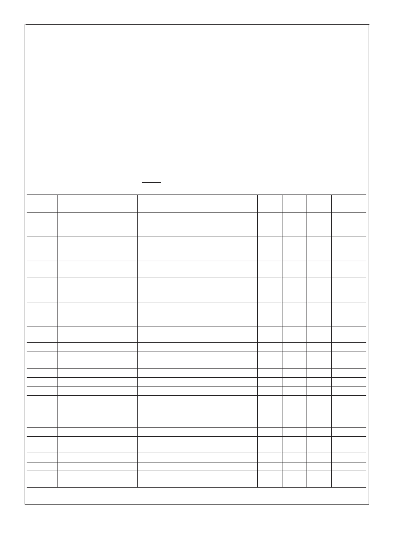
Electrical Characteristics
Test Circuit, T = 25C, all switches open, RESET to V
S
unless otherwise noted
(Notes 1, 2)
Symbol
Parameter
Conditions
Min
Typ
Max
Units
(Limits)
I
S
Supply Current
V
S
= 1.5V
V
S
= 5V
V
S
= 12V
V
S
= 1.5V
V
S
= 5V
V
S
= 12V
V
S
= 1.5V, I
DIS
= 1 mA
V
S
= 5V, I
DIS
= 10 mA
V
S
= 1.5V, I
O
= 1 mA
V
S
= 5V, I
O
= 8 mA
V
S
= 12V, I
O
= 50 mA
V
S
= 1.5V, I
O
= 0.25 mA
V
S
= 5V, I
O
= 2 mA
V
S
= 12V, I
O
= 10 mA
V
S
= 1.5V
V
S
= 12V
V
S
= 5V
V
S
= 1.5V (Note 4)
V
S
= 12V
V
S
= 5V
V
S
= 5V
V
S
= 12V
SW 2, 4 Closed
V
S
= 1.5V
V
S
= 5V
V
S
= 12V
V
S
= 5V
±
1V
V
S
= 5V
40C
≤
T
≤
+85C
SW 1, 3 Closed, V
S
= 12V
Max. Freq. Test Circuit, V
S
= 5V
Max. Freq. Test Circuit
V
S
= 5V, C
L
= 10 pF
50
100
150
1.0
3.3
8.0
75
150
0.2
0.3
1.0
1.25
4.7
11.3
0.5
4.0
10
0.7
0.75
10
10
1.0
150
250
400
1.2
3.8
8.6
150
300
0.4
0.6
2.0
μA
V
CTRL
Control Voltage
0.8
2.9
7.4
V
V
DIS
Discharge Saturation
Voltage
Output Voltage (Low)
mV
V
OL
V
V
OH
Output Voltage
(High)
1.0
4.4
10.5
0.4
3.7
V
V
TRIG
Trigger Voltage
0.6
4.3
V
I
TRIG
V
RES
Trigger Current
Reset Voltage
pA
0.4
0.4
1.0
1.1
V
I
RES
I
THRESH
I
DIS
t
Reset Current
Threshold Current
Discharge Leakage
Timing Accuracy
pA
pA
nA
100
0.9
1.0
1.0
1.1
1.1
1.1
0.3
75
1.25
1.20
1.25
ms
t/
V
S
t/
T
Timing Shift with Supply
Timing Shift with
Temperature
Astable Frequency
Maximum Frequency
Output Rise and
Fall Times
%/V
ppm/C
f
A
f
MAX
t
R
, t
F
4.0
4.8
3.0
15
5.6
kHz
MHz
ns
L
www.national.com
3
相關(guān)PDF資料 |
PDF描述 |
|---|---|
| LMC555CMMX | CMOS Timer |
| LMC555CMX | CMOS Timer |
| LMC555CBP | CMOS Timer |
| LMC555CBPX | CMOS Timer |
| LMC567 | Low Power Tone Decoder |
相關(guān)代理商/技術(shù)參數(shù) |
參數(shù)描述 |
|---|---|
| LMC555CMM | 制造商:Texas Instruments 功能描述:IC CMOS TIMER SMD MSOP8 555 |
| LMC555CMM/NOPB | 功能描述:計(jì)時器和支持產(chǎn)品 CMOS TIMER RoHS:否 制造商:Micrel 類型:Standard 封裝 / 箱體:SOT-23 內(nèi)部定時器數(shù)量:1 電源電壓-最大:18 V 電源電壓-最小:2.7 V 最大功率耗散: 最大工作溫度:+ 85 C 最小工作溫度:- 40 C 封裝:Reel |
| LMC555CMMX | 功能描述:計(jì)時器和支持產(chǎn)品 RoHS:否 制造商:Micrel 類型:Standard 封裝 / 箱體:SOT-23 內(nèi)部定時器數(shù)量:1 電源電壓-最大:18 V 電源電壓-最小:2.7 V 最大功率耗散: 最大工作溫度:+ 85 C 最小工作溫度:- 40 C 封裝:Reel |
| LMC555CMMX/NOPB | 功能描述:計(jì)時器和支持產(chǎn)品 RoHS:否 制造商:Micrel 類型:Standard 封裝 / 箱體:SOT-23 內(nèi)部定時器數(shù)量:1 電源電壓-最大:18 V 電源電壓-最小:2.7 V 最大功率耗散: 最大工作溫度:+ 85 C 最小工作溫度:- 40 C 封裝:Reel |
| LMC555CMNOPB | 制造商:Texas Instruments 功能描述: |
發(fā)布緊急采購,3分鐘左右您將得到回復(fù)。