- 您現(xiàn)在的位置:買賣IC網(wǎng) > PDF目錄385488 > LM883AH (National Semiconductor Corporation) Operational Amplifier PDF資料下載
參數(shù)資料
| 型號: | LM883AH |
| 廠商: | National Semiconductor Corporation |
| 英文描述: | Operational Amplifier |
| 中文描述: | 運算放大器 |
| 文件頁數(shù): | 2/8頁 |
| 文件大小: | 227K |
| 代理商: | LM883AH |
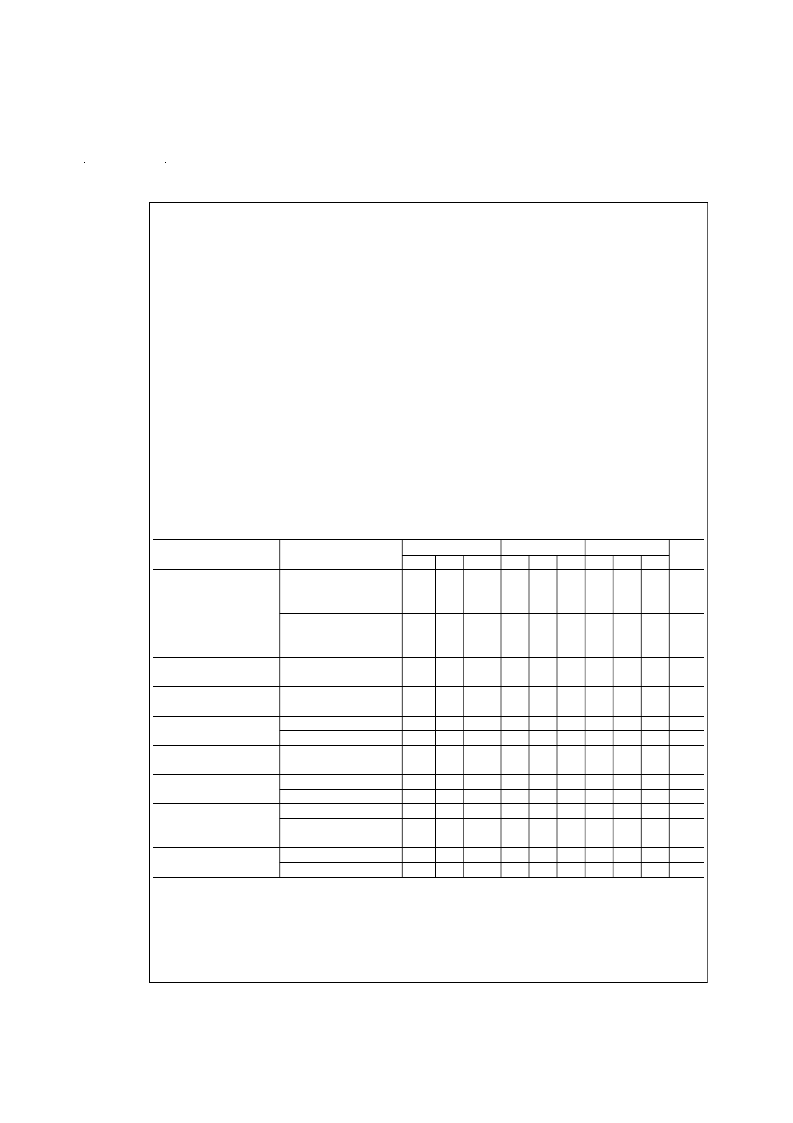
Absolute Maximum Ratings
(Note 1)
If Military/Aerospace specified devices are required, please contact the National Semiconductor Sales Office/
Distributors for availability and specifications.
(Note 6)
LM741A
±
22V
500 mW
±
30V
±
15V
Continuous
55C to +125C
65C to +150C
150C
LM741E
±
22V
500 mW
±
30V
±
15V
Continuous
0C to +70C
65C to +150C
100C
LM741
±
22V
500 mW
±
30V
±
15V
Continuous
55C to +125C
65C to +150C
150C
LM741C
±
18V
500 mW
±
30V
±
15V
Continuous
0C to +70C
65C to +150C
100C
Supply Voltage
Power Dissipation (Note 2)
Differential Input Voltage
Input Voltage (Note 3)
Output Short Circuit Duration
Operating Temperature Range
Storage Temperature Range
Junction Temperature
Soldering Information
N-Package (10 seconds)
J- or H-Package (10 seconds)
M-Package
Vapor Phase (60 seconds)
Infrared (15 seconds)
See AN-450 “Surface Mounting Methods and Their Effect on Product Reliability” for other methods of soldering
surface mount devices.
ESD Tolerance (Note 7)
400V
260C
300C
260C
300C
260C
300C
260C
300C
215C
215C
215C
215C
215C
215C
215C
215C
400V
400V
400V
Electrical Characteristics
(Note 4)
Parameter
Conditions
LM741A/LM741E
Min
Typ
LM741
Typ
LM741C
Typ
Units
Max
Min
Max
Min
Max
Input Offset Voltage
T
A
= 25C
R
S
≤
10 k
R
S
≤
50
T
AMIN
≤
T
A
≤
T
AMAX
R
S
≤
50
R
S
≤
10 k
1.0
5.0
2.0
6.0
mV
mV
0.8
3.0
4.0
mV
mV
μV/C
6.0
7.5
Average Input Offset
Voltage Drift
Input Offset Voltage
Adjustment Range
Input Offset Current
15
T
A
= 25C, V
S
=
±
20V
±
10
±
15
±
15
mV
T
A
= 25C
T
AMIN
≤
T
A
≤
T
AMAX
3.0
30
70
0.5
20
85
200
500
20
200
300
nA
nA
Average Input Offset
Current Drift
Input Bias Current
nA/C
T
A
= 25C
T
AMIN
≤
T
A
≤
T
AMAX
T
A
= 25C, V
S
=
±
20V
T
AMIN
≤
T
A
≤
T
AMAX
,
V
S
=
±
20V
T
A
= 25C
T
AMIN
≤
T
A
≤
T
AMAX
30
80
80
500
1.5
80
500
0.8
nA
μA
M
M
0.210
Input Resistance
1.0
0.5
6.0
0.3
2.0
0.3
2.0
Input Voltage Range
±
12
±
13
V
V
±
12
±
13
www.national.com
2
相關(guān)PDF資料 |
PDF描述 |
|---|---|
| LM883AJ-14 | Operational Amplifier |
| LM883H | Operational Amplifier |
| LM883J | Operational Amplifier |
| LM883J-14 | Operational Amplifier |
| LM883W | Operational Amplifier |
相關(guān)代理商/技術(shù)參數(shù) |
參數(shù)描述 |
|---|---|
| LM883AJ | 制造商:NSC 制造商全稱:National Semiconductor 功能描述:Low Power Quad Operational Amplifiers |
| LM883AJ-14 | 制造商:NSC 制造商全稱:National Semiconductor 功能描述:Operational Amplifier |
| LM883AW | 制造商:NSC 制造商全稱:National Semiconductor 功能描述:Low Power Quad Operational Amplifiers |
| LM883AWG | 制造商:NSC 制造商全稱:National Semiconductor 功能描述:Low Power Quad Operational Amplifiers |
| LM883E | 制造商:NSC 制造商全稱:National Semiconductor 功能描述:3-Terminal Adjustable Regulator |
發(fā)布緊急采購,3分鐘左右您將得到回復(fù)。