- 您現(xiàn)在的位置:買賣IC網(wǎng) > PDF目錄361035 > LM837MX Voltage-Feedback Operational Amplifier PDF資料下載
參數(shù)資料
| 型號: | LM837MX |
| 元件分類: | 運算放大器 |
| 英文描述: | Voltage-Feedback Operational Amplifier |
| 中文描述: | 電壓反饋運算放大器 |
| 文件頁數(shù): | 2/8頁 |
| 文件大小: | 414K |
| 代理商: | LM837MX |
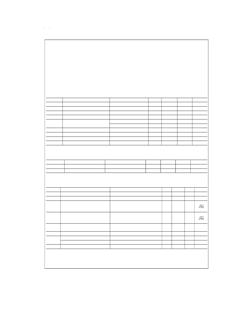
Absolute Maximum Ratings
(Note 1)
If Military/Aerospace specified devices are required,
please contact the National Semiconductor Sales Office/
Distributors for availability and specifications.
Supply Voltage, V
CC
/V
EE
Differential Input Voltage, V
ID
(Note 2)
Common Mode Input Voltage, V
IC
(Note 2)
Power Dissipation, P
D
(Note 3)
±
18V
±
30V
±
15V
1.2W (N)
830 mW (M)
40C to +85C
Operating Temperature Range, T
OPR
Storage Temperature Range, T
STG
Soldering Information
Dual-In-Line Package
Soldering (10 seconds)
Small Outline Package
Vapor Phase (60 seconds)
Infrared (15 seconds)
ESD rating to be determined.
See AN-450 “Surface Mounting Methods and Their Effect
on Product Reliability” for other methods of soldering
surface mount devices.
60C to +150C
260C
215C
220C
DC Electrical Characteristics
T
A
= 25C, V
S
=
±
15V
Symbol
V
OS
Input Offset Voltage
I
OS
Input Offset Current
I
B
Input Bias Current
A
V
Large Signal Voltage Gain
V
OM
Output Voltage Swing
Parameter
Condition
Min
Typ
0.3
10
500
110
±
13.5
±
12.5
±
14.0
100
100
10
Max
5
200
1000
Units
mV
nA
nA
dB
V
V
V
dB
dB
mA
R
S
= 50
R
L
= 2 k
, V
OUT
=
±
10V
R
L
= 2 k
R
L
= 600
90
±
12
±
10
±
12
80
80
V
CM
CMRR
PSRR
I
S
Common Mode Input Voltage
Common Mode Rejection Ratio
Power Supply Rejection Ratio
Power Supply Current
V
IN
=
±
12V
V
S
= 15
z
5, 15
z
5
R
L
=
∞
, Four Amps
15
AC Electrical Characteristics
T
A
= 25C, V
S
=
±
15V
Symbol
Parameter
SR
Slew Rate
GBW
Gain Bandwidth Product
Condition
Min
8
15
Typ
10
25
Max
Units
V/μs
MHz
R
L
= 600
f = 100 kHz, R
L
= 600
Design Electrical Characteristics
T
A
= 25C, V
S
=
±
15V (Note 4)
Symbol
Parameter
PBW
Power Bandwidth
e
n1
Equivalent Input Noise Voltage
e
n2
Equivalent Input Noise Voltage
Condition
Min
Typ
200
0.5
Max
Units
kHz
μV
nV/
V
O
= 25 V
P-P
, R
L
= 600
, THD
<
1%
JIS A, R
S
= 100
f = 1 kHz
4.5
i
n
Equivalent Input Noise Current
f = 1 kHz
0.7
pA/
THD
Total Harmonic Distortion
A
= 1, V
OUT
= 3 Vrms,
f = 20
z
20 kHz, R
L
= 600
Open Loop
Open Loop
f = 20
z
20 kHz
0.0015
%
f
U
φ
m
Zero Cross Frequency
Phase Margin
Input-Referred Crosstalk
Average TC of Input Offset Voltage
12
45
MHz
deg
dB
μV/C
120
2
V
OS
/
T
Note 1:
Absolute Maximum Ratings indicate limits beyond which damage to the device may occur. Operating Ratings indicate conditions for which the device is func-
tional, but do not guarantee specific performance limits. Electrical Characteristics state DC andAC electrical specifications under particular test conditions which guar-
antee specific performance limits. This assumes that the device is within the Operating Ratings. Specifications are not guaranteed for parameters where no limit is
given, however, the typical value is a good indication of device performance.
Note 2:
Unless otherwise specified the absolute maximum input voltage is equal to the power supply voltage.
www.national.com
2
相關(guān)PDF資料 |
PDF描述 |
|---|---|
| LM837M | Low Noise Quad Operational Amplifier |
| LM837N | Low Noise Quad Operational Amplifier |
| LM84CIMQAX | Diode Input Digital Temperature Sensor with Two-Wire Interface |
| LM84 | Diode Input Digital Temperature Sensor with Two-Wire Interface |
| LM84CIMQA | Diode Input Digital Temperature Sensor with Two-Wire Interface |
相關(guān)代理商/技術(shù)參數(shù) |
參數(shù)描述 |
|---|---|
| LM837MX/NOPB | 功能描述:運算放大器 - 運放 RoHS:否 制造商:STMicroelectronics 通道數(shù)量:4 共模抑制比(最小值):63 dB 輸入補(bǔ)償電壓:1 mV 輸入偏流(最大值):10 pA 工作電源電壓:2.7 V to 5.5 V 安裝風(fēng)格:SMD/SMT 封裝 / 箱體:QFN-16 轉(zhuǎn)換速度:0.89 V/us 關(guān)閉:No 輸出電流:55 mA 最大工作溫度:+ 125 C 封裝:Reel |
| LM837N | 制造商:Texas Instruments 功能描述:IC OP AMP QUAD DIP14 837 |
| LM837N | 制造商:Texas Instruments 功能描述:IC OP AMP QUAD DIP14 837 |
| LM837N/A+ | 制造商:未知廠家 制造商全稱:未知廠家 功能描述:Voltage-Feedback Operational Amplifier |
| LM837N/B+ | 制造商:未知廠家 制造商全稱:未知廠家 功能描述:Voltage-Feedback Operational Amplifier |
發(fā)布緊急采購,3分鐘左右您將得到回復(fù)。