- 您現(xiàn)在的位置:買賣IC網(wǎng) > PDF目錄361033 > LM723 (NATIONAL SEMICONDUCTOR CORP) Voltage Regulator PDF資料下載
參數(shù)資料
| 型號(hào): | LM723 |
| 廠商: | NATIONAL SEMICONDUCTOR CORP |
| 元件分類: | 基準(zhǔn)電壓源/電流源 |
| 英文描述: | Voltage Regulator |
| 中文描述: | 2 V-37 V ADJUSTABLE POSITIVE REGULATOR, UUC14 |
| 封裝: | DIE-14 |
| 文件頁(yè)數(shù): | 3/14頁(yè) |
| 文件大?。?/td> | 470K |
| 代理商: | LM723 |
第1頁(yè)第2頁(yè)當(dāng)前第3頁(yè)第4頁(yè)第5頁(yè)第6頁(yè)第7頁(yè)第8頁(yè)第9頁(yè)第10頁(yè)第11頁(yè)第12頁(yè)第13頁(yè)第14頁(yè)
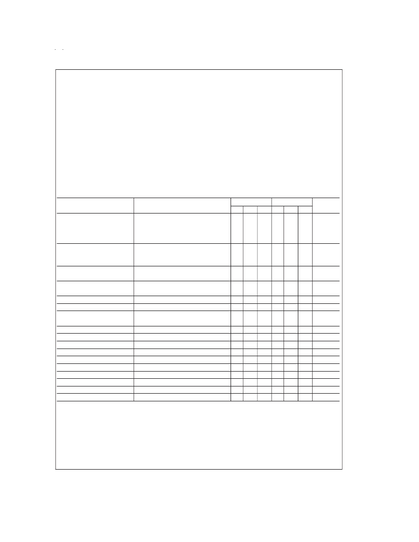
Absolute Maximum Ratings
(Note 1)
If Military/Aerospace specified devices are required,
please contact the National Semiconductor Sales Office/
Distributors for availability and specifications.
(Note 10)
Pulse Voltage from V
+
to V
(50 ms)
Continuous Voltage from V
+
to V
Input-Output Voltage Differential
Maximum Amplifier Input Voltage
(Either Input)
Maximum Amplifier Input Voltage
(Differential)
Current from V
Z
Current from V
REF
Internal Power Dissipation
Metal Can (Note 2)
50V
40V
40V
8.5V
5V
25 mA
15 mA
800 mW
Cavity DIP (Note 2)
Molded DIP (Note 2)
Operating Temperature Range
LM723
LM723C
Storage Temperature Range
Metal Can
Molded DIP
Lead Temperature (Soldering, 4 sec. max.)
Hermetic Package
Plastic Package
ESD Tolerance
(Human body model, 1.5 k
in series with 100 pF)
900 mW
660 mW
55C to +150C
0C to +70C
65C to +150C
55C to +150C
300C
260C
1200V
Electrical Characteristics
(Note 3) (Note 10)
Parameter
Conditions
LM723
Typ
0.01
LM723C
Typ
0.01
Units
Min
Max
0.1
0.3
Min
Max
0.1
Line Regulation
V
IN
= 12V to V
IN
= 15V
55C
≤
T
A
≤
+125C
0C
≤
T
A
≤
+70C
V
IN
= 12V to V
IN
= 40V
I
L
= 1 mA to I
L
= 50 mA
55C
≤
T
A
≤
+125C
0C
≤
T
A
≤
+70C
f = 50 Hz to 10 kHz, C
REF
= 0
f = 50 Hz to 10 kHz, C
REF
= 5 μF
55C
≤
T
A
≤
+125C
0C
≤
T
A
≤
+70C
R
SC
= 10
, V
OUT
= 0
% V
OUT
% V
OUT
% V
OUT
% V
OUT
% V
OUT
% V
OUT
% V
OUT
dB
dB
%/C
%/C
mA
V
μVrms
μVrms
%/1000 hrs
mA
V
V
V
C/W
C/W
C/W
C/W
C/W
0.3
0.5
0.2
0.02
0.03
0.2
0.15
0.6
0.1
0.03
Load Regulation
0.6
Ripple Rejection
74
86
74
86
Average Temperature Coeffic-
ient of Output Voltage (Note 8)
Short Circuit Current Limit
Reference Voltage
Output Noise Voltage
0.002 0.015
0.003 0.015
65
65
6.95 7.15
7.35 6.80 7.15
7.50
BW = 100 Hz to 10 kHz, C
REF
= 0
BW = 100 Hz to 10 kHz, C
REF
= 5 μF
86
2.5
0.05
1.7
86
2.5
0.05
1.7
Long Term Stability
Standby Current Drain
Input Voltage Range
Output Voltage Range
Input-Output Voltage Differential
θ
JA
θ
JA
θ
JA
θ
JA
θ
JC
I
L
= 0, V
IN
= 30V
3.5
40
37
38
4.0
40
37
38
9.5
2.0
3.0
9.5
2.0
3.0
Molded DIP
Cavity DIP
H10C Board Mount in Still Air
H10C Board Mount in 400 LF/Min Air Flow
105
150
165
66
22
165
66
22
Note 1:
“Absolute Maximum Ratings” indicate limits beyond which damage to the device may occur. Operating Ratings indicate conditions for which the device is
functional, but do not guarantee specific performance limits.
Note 2:
See derating curves for maximum power rating above 25C.
Note 3:
Unless otherwise specified, T
= 25C, V
= V
+
= V
= 12V, V
= 0, V
= 5V, I
= 1 mA, R
= 0, C
= 100 pF, C
= 0 and divider impedance as
seen by error amplifier
≤
10 k
connected as shown in Figure 1 Line and load regulation specifications are given for the condition of constant chip temperature. Tem-
perature drifts must be taken into account separately for high dissipation conditions.
Note 4:
L
1
is 40 turns of No. 20 enameled copper wire wound on Ferroxcube P36/22-3B7 pot core or equivalent with 0.009 in. air gap.
Note 5:
Figures in parentheses may be used if R1/R2 divider is placed on opposite input of error amp.
Note 6:
Replace R1/R2 in figures with divider shown in Figure 13
Note 7:
V
+
and V
CC
must be connected to a +3V or greater supply.
Note 8:
For metal can applications where V
Z
is required, an external 6.2V zener diode should be connected in series with V
OUT
.
www.national.com
3
相關(guān)PDF資料 |
PDF描述 |
|---|---|
| LM723CJ | Positive Adjustable Voltage Regulator |
| LM723ID | Positive Adjustable Voltage Regulator |
| LM723IN | Positive Adjustable Voltage Regulator |
| LM723J | Positive Adjustable Voltage Regulator |
| LM723 | HIGH PRECISION VOLTAGE REGULATOR |
相關(guān)代理商/技術(shù)參數(shù) |
參數(shù)描述 |
|---|---|
| LM723_07 | 制造商:STMICROELECTRONICS 制造商全稱:STMicroelectronics 功能描述:High precision voltage regulator |
| LM723C | 制造商:STMICROELECTRONICS 制造商全稱:STMicroelectronics 功能描述:HIGH PRECISION VOLTAGE REGULATOR |
| LM723CD | 功能描述:線性穩(wěn)壓器 - 標(biāo)準(zhǔn) 2.0-37V Programable RoHS:否 制造商:STMicroelectronics 輸出類型: 極性: 輸出電壓:1.8 V 輸出電流:150 mA 負(fù)載調(diào)節(jié): 最大輸入電壓:5.5 V 線路調(diào)整率: 最大工作溫度:+ 125 C 安裝風(fēng)格:SMD/SMT 封裝 / 箱體:SOT-323-5L |
| LM723CD013TR | 功能描述:線性穩(wěn)壓器 - 標(biāo)準(zhǔn) 2.0-37V Programable RoHS:否 制造商:STMicroelectronics 輸出類型: 極性: 輸出電壓:1.8 V 輸出電流:150 mA 負(fù)載調(diào)節(jié): 最大輸入電壓:5.5 V 線路調(diào)整率: 最大工作溫度:+ 125 C 安裝風(fēng)格:SMD/SMT 封裝 / 箱體:SOT-323-5L |
| LM723CH | 功能描述:線性穩(wěn)壓器 - 標(biāo)準(zhǔn) RoHS:否 制造商:STMicroelectronics 輸出類型: 極性: 輸出電壓:1.8 V 輸出電流:150 mA 負(fù)載調(diào)節(jié): 最大輸入電壓:5.5 V 線路調(diào)整率: 最大工作溫度:+ 125 C 安裝風(fēng)格:SMD/SMT 封裝 / 箱體:SOT-323-5L |
發(fā)布緊急采購(gòu),3分鐘左右您將得到回復(fù)。