- 您現(xiàn)在的位置:買賣IC網(wǎng) > PDF目錄30757 > LM7131BMWC (NATIONAL SEMICONDUCTOR CORP) 1 CHANNEL, VIDEO AMPLIFIER, UUC PDF資料下載
Notes on Performance Curves and Datasheet Limits (Continued)
DRIVING TYPE 1175 FLASH A/D LOADS
The circuits in
Figures 6, 7, 8, 9, 10, 11 show a LM7131 in a
voltage follower configuration driving the passive equivalent
of a typical flash A/D input. Note that there is a slight ringing
on the output, which can affect accurate analog-to-digital
conversion. In these graphs, we have adjusted the ringing to
be a little larger than desirable in order to better show the
settling time. Most settling times at low gain are about 75 ns
to < 1% of final voltage. The ringing can be reduced by add-
ing a low value (approximately 500
) feedback resistor from
the output to the inverting input and placing a small (pico-
farad range) capacitor across the feedback resistor. See
Fig-
ure 9 and Figure 10 for schematics and respective perfor-
mance curves for flash A/D driving at A
V = +5 with and
withouta2pF feedback capacitor.
See section on feedback compensation. Ringing can also be
reduced by placing an isolation resistor between the output
and the analog-to-digital converter input — see sections on
driving capacitive loads and analog-to-digital converters.
Please refer to
Figures 6, 7, 8, 9, 10, 11 for schematics of
test setups for driving flash A/D converters.
DS012313-12
Numbers in parentheses are measured
fixture capacitances w/o DUT and load.
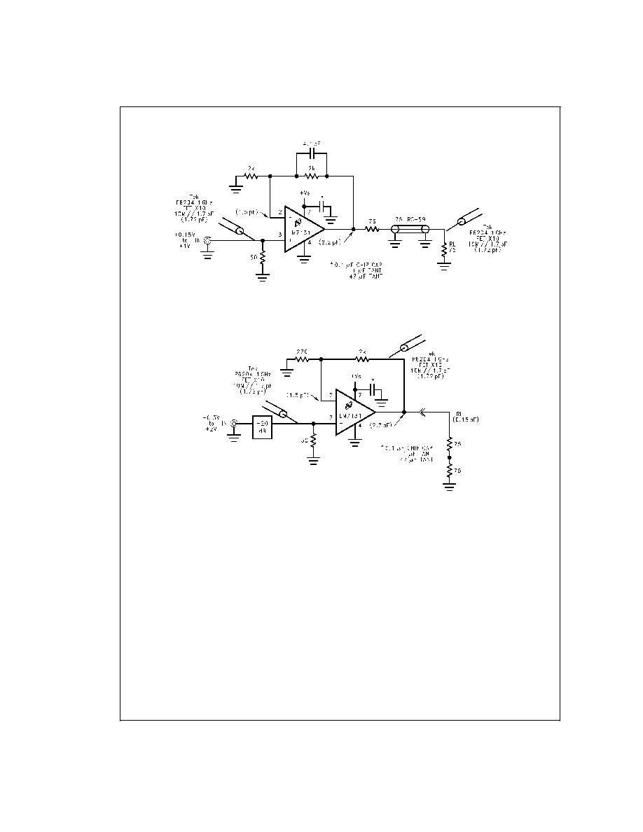
FIGURE 4. Cable Driver 75' RG-59
DS012313-13
Numbers in parentheses are measured
fixture capacitances w/o DUT and load.
FIGURE 5. Cable Driver Gain of 10 A
V = +10
www.national.com
12
相關PDF資料 |
PDF描述 |
|---|---|
| LM733H/883C | 1 CHANNEL, VIDEO AMPLIFIER, MBCY10 |
| LM733H/883 | 1 CHANNEL, VIDEO AMPLIFIER, MBCY10 |
| LM809-4.38MDC | 1-CHANNEL POWER SUPPLY SUPPORT CKT, UUC |
| LM809-2.93MDC | 1-CHANNEL POWER SUPPLY SUPPORT CKT, UUC |
| LM809-4.00MWC | 1-CHANNEL POWER SUPPLY SUPPORT CKT, UUC |
相關代理商/技術參數(shù) |
參數(shù)描述 |
|---|---|
| LM714 | 制造商:未知廠家 制造商全稱:未知廠家 功能描述:Analog IC |
| LM715 | 制造商:NSC 制造商全稱:National Semiconductor 功能描述:High Speed Operational Amplifier |
| LM7152 | 制造商:未知廠家 制造商全稱:未知廠家 功能描述:Telecommunication IC |
| LM7152M | 制造商:未知廠家 制造商全稱:未知廠家 功能描述:Telecommunication IC |
| LM715CH | 制造商:NSC 制造商全稱:National Semiconductor 功能描述:High Speed Operational Amplifier |
發(fā)布緊急采購,3分鐘左右您將得到回復。