- 您現在的位置:買賣IC網 > PDF目錄385488 > LM6310IMX (NATIONAL SEMICONDUCTOR CORP) High Speed Low Power Operational Amplifier with TRI-STATE Output PDF資料下載
參數資料
| 型號: | LM6310IMX |
| 廠商: | NATIONAL SEMICONDUCTOR CORP |
| 元件分類: | 運動控制電子 |
| 英文描述: | High Speed Low Power Operational Amplifier with TRI-STATE Output |
| 中文描述: | OP-AMP, 9000 uV OFFSET-MAX, PDSO8 |
| 封裝: | SOP-8 |
| 文件頁數: | 3/16頁 |
| 文件大小: | 279K |
| 代理商: | LM6310IMX |
g
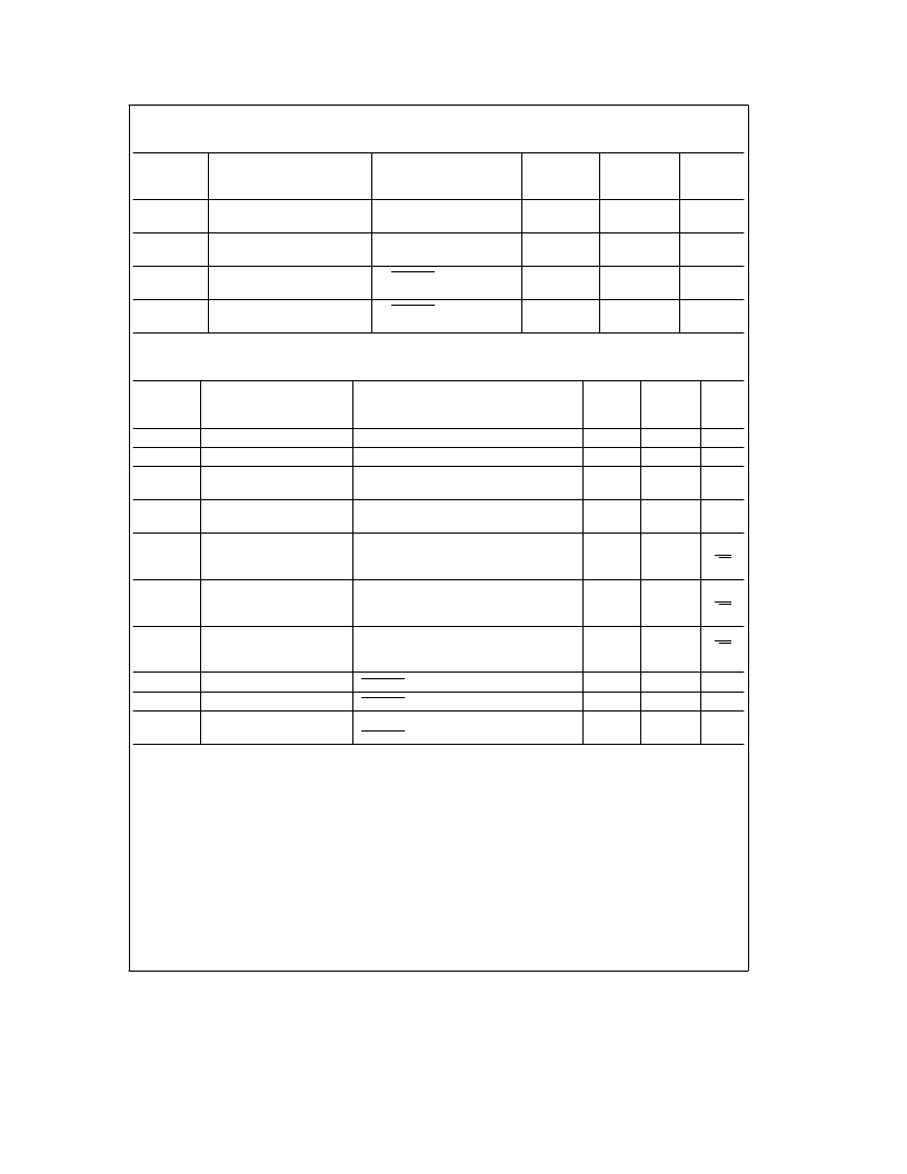
5V DC Electrical Characteristics
Unless otherwise specified, all limits guaranteed for T
J
e
25
§
C, V
a
e
5V, V
b
e b
5V, V
CM
e
V
O
e
0V and R
L
e
100
X
.
Boldface
limits apply at the temperature extremes (Continued)
Typ
LM6310I
Limit
(Note 6)
Symbol
Parameter
Conditions
(Note 5)
Units
I
SC
Output Current
10
X
to 0V
Sourcing
60
44
20
mA
min
R
OUT
Output Resistance
Closed Loop
0.06
X
max
I
S
Supply Current for
Normal Operation Mode
DISABLE (Pin 8)
l
2.0V
3.5
4.5
5.0
mA
max
I
S
Supply Current Powerdown
(TRI-STATE) Mode
DISABLE (Pin 8)
k
0.8V
0.8
1.0
1.2
mA
max
g
5V AC Electrical Characteristics
Unless otherwise specified, all limits guaranteed for T
J
e
25
§
C, V
a
e
5V, V
b
e b
5V, V
CM
e
V
O
e
0V and R
L
e
100
X
.
Boldface
limits apply at the temperature extremes
Typ
LM6310I
Limit
(Note 6)
Symbol
Parameter
Conditions
(Note 5)
Units
SR
Slew Rate
A
V
e a
2, 2V Output Pulse
300
V/
m
s
b
3 dB BW
b
3db Bandwidth
A
V
e a
2
90
MHz
Dg
Differential Gain
(Note 7)
A
V
e a
2, 150
X
Load (75
X
Back-Terminated)
1 k
X
Pull-Down to
b
5V on Output
0.05
%
Dp
Differential Phase
(Note 7)
A
V
e a
2, 150
X
Load (75
X
Back-Terminated)
1 k
X
Pull-Down to
b
5V on Output
0.33
§
e
n
Input-Referred
Voltage Noise
f
e
1 MHz
5
nV
0
Hz
Input-Referred Current Noise
Non-Inverting (
b
) Input
f
e
1 MHz
3
pA
0
Hz
Input-Referred Current
Noise Inverting (
b
) Input
f
e
1 MHz
12
pA
0
Hz
t
ON
Turn On Time
DISABLE (Pin 8) Low to High
50
ns
t
OFF
Turn Off Time
DISABLE (Pin 8) High to Low
25
ns
Output Isolation
Output Isolation from Inputs when
DISABLE
e
Low 10 MHz
55
db
Note 1:
Absolute Maximum Ratings indicate limits beyond which damage to the device may occur. Operating Ratings indicate conditions for which the device is
intended to be functional, but specific performance is not guaranteed. For guaranteed specifications and the test conditions, see the Electrical characteristics.
Note 2:
Human body model, 1.5 k
X
in series with 100 pF.
Note 3:
Applies to both single-supply and split-supply operation. Continuous short circuit operation at elevated ambient temperature can result in exceeding the
maximum allowed junction temperature of 150
§
C.
Note 4:
The maximum power dissipation is a function of T
J(max)
,
i
JA
, and T
A
. The maximum allowable power dissipation at any ambient temperature is P
D
e
(T
J(max)
–T
A
)/
i
JA
. All numbers apply for packages soldered directly into a PC board.
Note 5:
Typical values represent the most likely parametric norm.
Note 6:
All limits are guaranteed by testing or statistical analysis.
Note 7:
Differential Gain and Phase performance is sensitive to layout. Follow layout suggestions in text for best results.
http://www.national.com
3
相關PDF資料 |
PDF描述 |
|---|---|
| LM6310IN | High Speed Low Power Operational Amplifier with TRI-STATE Output |
| LM64 | 【1∑C Remote Diode Temperature Sensor with PWM Fan Control and 5 GPIO’s |
| LM6584 | TFT-LCD Quad, 13V RRIO High Output Current |
| LM6584MA | TFT-LCD Quad, 13V RRIO High Output Current |
| LM6584MAX | TFT-LCD Quad, 13V RRIO High Output Current |
相關代理商/技術參數 |
參數描述 |
|---|---|
| LM6310IN | 制造商:NSC 制造商全稱:National Semiconductor 功能描述:High Speed Low Power Operational Amplifier with TRI-STATE Output |
| LM6311 | 制造商:未知廠家 制造商全稱:未知廠家 功能描述: |
| LM6311IN | 制造商:TI 制造商全稱:Texas Instruments 功能描述:Low Noise High Speed Voltage Feedback Operational Amplifier |
| LM6313 | 制造商:NSC 制造商全稱:National Semiconductor 功能描述:High Power Operational Amplifier |
| LM6313N | 制造商:NSC 制造商全稱:National Semiconductor 功能描述:High Power Operational Amplifier |
發(fā)布緊急采購,3分鐘左右您將得到回復。