- 您現(xiàn)在的位置:買賣IC網(wǎng) > PDF目錄358871 > LM621N (NATIONAL SEMICONDUCTOR CORP) LM621 Brushless Motor Commutator PDF資料下載
參數(shù)資料
| 型號: | LM621N |
| 廠商: | NATIONAL SEMICONDUCTOR CORP |
| 元件分類: | 運(yùn)動控制電子 |
| 英文描述: | LM621 Brushless Motor Commutator |
| 中文描述: | BRUSHLESS DC MOTOR CONTROLLER, PDIP18 |
| 封裝: | PLASTIC, DIP-18 |
| 文件頁數(shù): | 8/12頁 |
| 文件大?。?/td> | 224K |
| 代理商: | LM621N |
Dead-Time Feature
(Continued)
Dead-time is defined as the time the outputs are blanked off
(to prevent shoot-through currents) after a direction change
input. SeeFigure 3. It can be seen that the dead-time is two
clock periods. Since the dead-time scheme introduces de-
lay into the system feedback control loop, which could im-
pact system performance or stability, it is important that the
dead-time be kept to a minimum. From Figure 3 it can be
seen that the time between a direction change signal and
the initiation of output blanking can vary up to one clock
period due to asynchronous nature of the clock and the
direction signal.
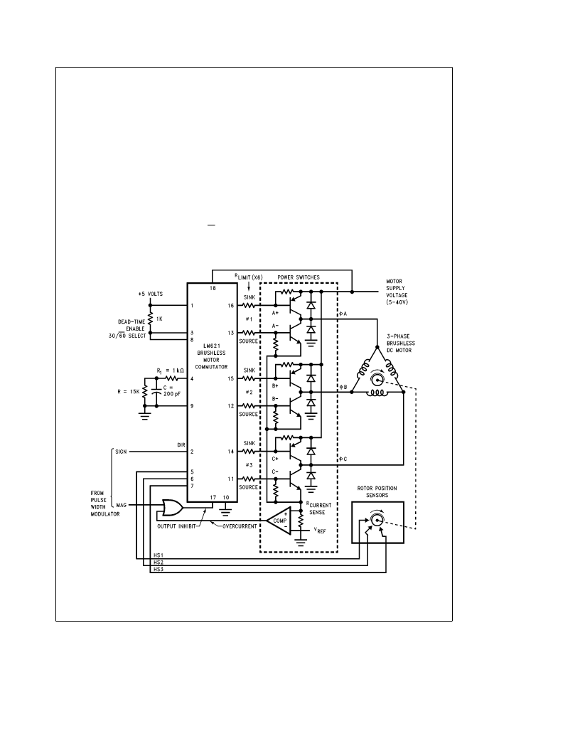
Typical Applications
THREE-PHASE EXAMPLES
Figure 4 is a typical LM621 application. This circuitry is for
use with a three-phase motor having 30-degree sensor
phasing, as indicated by connection of the 30/60 SELECT
input, pin 8, to a logic ‘‘1’’ (
a
5V). The same connection of
the DEAD-TIME ENABLE input, pin 3, enables this feature.
Typical power switches and a simple implementation of an
overcurrent sensing circuit are also detailed inFigure 4. This
application example assumes a device turn-off time of about
4.8
m
s maximum, as evidenced by the choice of R and C.
See Typical Performance Characteristics. The choice of RC
should be made such that two periods are at least equal to
the maximum device turn-off time.
The choice of the value for R
limit
(the resistors which couple
the LM621 outputs to the power switches) depends on the
input current requirements of the power switching devices.
These resistors should be chosen to provide only the
amount of current needed by the device inputs, up to 50 mA
(typical). The resistors minimize the dissipation incurred by
the LM621. AlthoughFigure 4 shows the 5–40V supply (pin
18) connected to the motor supply voltage, this was done
only to emphasize the ability of the part to provide up to 40V
output swings. For the bipolar power switches shown, con-
necting pin 18 to a 5V supply would reduce on-chip power
dissipation. Driving FET power switches, however, may re-
quire connecting pin 18 to a higher voltage. Figure 5 is the
three-phase application built with MOSFET power-switching
components. Note that since the output V
drop
(sourcing) is
at least 1.5V, V
CC2
can be chosen to avoid overdriving the
MOSFET gates.
TL/H/8679–9
FIGURE 4. Commutation of Three-Phase Motor (Bipolar Switches)
8
相關(guān)PDF資料 |
PDF描述 |
|---|---|
| LM6261 | High Speed Operational Amplifier |
| LM6261M | High Speed Operational Amplifier |
| LM6261N | High Speed Operational Amplifier |
| LM6264 | High Speed Operational Amplifier |
| LM6264N | High Speed Operational Amplifier |
相關(guān)代理商/技術(shù)參數(shù) |
參數(shù)描述 |
|---|---|
| LM621N/A+ | 制造商:未知廠家 制造商全稱:未知廠家 功能描述:DC Motor Controller/Driver |
| LM621N/B+ | 制造商:未知廠家 制造商全稱:未知廠家 功能描述:DC Motor Controller/Driver |
| LM6221 | 制造商:未知廠家 制造商全稱:未知廠家 功能描述: |
| LM6221H | 制造商:NSC 制造商全稱:National Semiconductor 功能描述:High Speed Buffer |
| LM6221N | 制造商:NSC 制造商全稱:National Semiconductor 功能描述:High Speed Buffer |
發(fā)布緊急采購,3分鐘左右您將得到回復(fù)。