- 您現(xiàn)在的位置:買賣IC網(wǎng) > PDF目錄358871 > LM621 (National Semiconductor Corporation) LM621 Brushless Motor Commutator PDF資料下載
參數(shù)資料
| 型號(hào): | LM621 |
| 廠商: | National Semiconductor Corporation |
| 英文描述: | LM621 Brushless Motor Commutator |
| 中文描述: | LM621無(wú)刷電機(jī)換向器 |
| 文件頁(yè)數(shù): | 7/12頁(yè) |
| 文件大?。?/td> | 224K |
| 代理商: | LM621 |
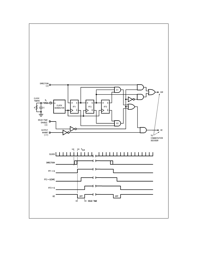
Dead-Time Feature
The DEAD-TIME ENABLE input is used to enable this fea-
ture (by connecting
a
5V to pin 3). The reason for providing
this feature is that the external power switches are usually
totem-pole structures. Since these structures switch heavy
currents, if either totem-pole device is not completely turned
off when its complementary device turns on, heavy ‘‘shoot-
through’’ current spiking will occur. This situation occurs
when the motor DIRECTION input changes (when all output
drive polarities reverse), at which time device turn-off delay
can cause the undesired current spiking.
Figure 2 shows the logic of the dead-time generator. The
dead-time generator includes an RC oscillator to generate a
required clock. Pin 4 (CLOCK TIMING) is used to connect
an external RC network to set the frequency of this oscilla-
tor. The clock frequency should be adjusted so that two
periods of oscillation just slightly exceed the worst-case
turn-off time of the power switching devices. As shown by
the graph in Typical Peformance Characteristics, the time of
one clock period (in
m
s) is approximately (0.756
c
10
3
)
(R
a
1) C, where R is in k
X
and C is in pF; the period can
be measured with an oscilloscope at pin 4. The dead-time
generator function monitors the DIRECTION input for
changes, synchronizes the direction changes with the inter-
nal clock, and inhibits the chip outputs for two clock periods.
Flip-flops FF1 through FF3 form a three-bit, shift-register
delay line, the input of which is the DIRECTION input. The
flip-flops are the only elements clocked by the internal clock
generator. The shift register outputs must all have the same
state in order to enable gate G1 or G2, one of which must
be enabled to enable the chip outputs. As soon as a direc-
tion change input is sensed at the output of FF1, gates G1
and G2 will be disabled, thereby disabling the drive to the
power switches for a time equal to two clock periods.
FIGURE 2. Dead-Time Generator Logic Diagram
TL/H/8679–7
TL/H/8679–8
FIGURE 3. Dead-Time Generator Waveforms
7
相關(guān)PDF資料 |
PDF描述 |
|---|---|
| LM6218AWMX | Voltage-Feedback Operational Amplifier |
| LM6218AWM | Voltage-Feedback Operational Amplifier |
| LM6218 | |
| LM621N | LM621 Brushless Motor Commutator |
| LM6261 | High Speed Operational Amplifier |
相關(guān)代理商/技術(shù)參數(shù) |
參數(shù)描述 |
|---|---|
| LM6211 | 制造商:NSC 制造商全稱:National Semiconductor 功能描述:Low Noise, RRO Operational Amplifier with CMOS Input and 24V Operation |
| LM6211MF | 功能描述:運(yùn)算放大器 - 運(yùn)放 RoHS:否 制造商:STMicroelectronics 通道數(shù)量:4 共模抑制比(最小值):63 dB 輸入補(bǔ)償電壓:1 mV 輸入偏流(最大值):10 pA 工作電源電壓:2.7 V to 5.5 V 安裝風(fēng)格:SMD/SMT 封裝 / 箱體:QFN-16 轉(zhuǎn)換速度:0.89 V/us 關(guān)閉:No 輸出電流:55 mA 最大工作溫度:+ 125 C 封裝:Reel |
| LM6211MF/NOPB | 功能描述:運(yùn)算放大器 - 運(yùn)放 Low Noise RRO Op Amp w/ CMOS Inpt 24V RoHS:否 制造商:STMicroelectronics 通道數(shù)量:4 共模抑制比(最小值):63 dB 輸入補(bǔ)償電壓:1 mV 輸入偏流(最大值):10 pA 工作電源電壓:2.7 V to 5.5 V 安裝風(fēng)格:SMD/SMT 封裝 / 箱體:QFN-16 轉(zhuǎn)換速度:0.89 V/us 關(guān)閉:No 輸出電流:55 mA 最大工作溫度:+ 125 C 封裝:Reel |
| LM6211MFX | 功能描述:運(yùn)算放大器 - 運(yùn)放 RoHS:否 制造商:STMicroelectronics 通道數(shù)量:4 共模抑制比(最小值):63 dB 輸入補(bǔ)償電壓:1 mV 輸入偏流(最大值):10 pA 工作電源電壓:2.7 V to 5.5 V 安裝風(fēng)格:SMD/SMT 封裝 / 箱體:QFN-16 轉(zhuǎn)換速度:0.89 V/us 關(guān)閉:No 輸出電流:55 mA 最大工作溫度:+ 125 C 封裝:Reel |
| LM6211MFX/NOPB | 功能描述:運(yùn)算放大器 - 運(yùn)放 RoHS:否 制造商:STMicroelectronics 通道數(shù)量:4 共模抑制比(最小值):63 dB 輸入補(bǔ)償電壓:1 mV 輸入偏流(最大值):10 pA 工作電源電壓:2.7 V to 5.5 V 安裝風(fēng)格:SMD/SMT 封裝 / 箱體:QFN-16 轉(zhuǎn)換速度:0.89 V/us 關(guān)閉:No 輸出電流:55 mA 最大工作溫度:+ 125 C 封裝:Reel |
發(fā)布緊急采購(gòu),3分鐘左右您將得到回復(fù)。