- 您現(xiàn)在的位置:買賣IC網(wǎng) > PDF目錄385488 > LM6211MF (NATIONAL SEMICONDUCTOR CORP) Low Noise, RRO Operational Amplifier with CMOS Input and 24V Operation PDF資料下載
參數(shù)資料
| 型號(hào): | LM6211MF |
| 廠商: | NATIONAL SEMICONDUCTOR CORP |
| 元件分類: | 運(yùn)動(dòng)控制電子 |
| 英文描述: | Low Noise, RRO Operational Amplifier with CMOS Input and 24V Operation |
| 中文描述: | OP-AMP, 2800 uV OFFSET-MAX, 17 MHz BAND WIDTH, PDSO5 |
| 封裝: | SOT-23, 5 PIN |
| 文件頁(yè)數(shù): | 12/19頁(yè) |
| 文件大?。?/td> | 1091K |
| 代理商: | LM6211MF |
第1頁(yè)第2頁(yè)第3頁(yè)第4頁(yè)第5頁(yè)第6頁(yè)第7頁(yè)第8頁(yè)第9頁(yè)第10頁(yè)第11頁(yè)當(dāng)前第12頁(yè)第13頁(yè)第14頁(yè)第15頁(yè)第16頁(yè)第17頁(yè)第18頁(yè)第19頁(yè)
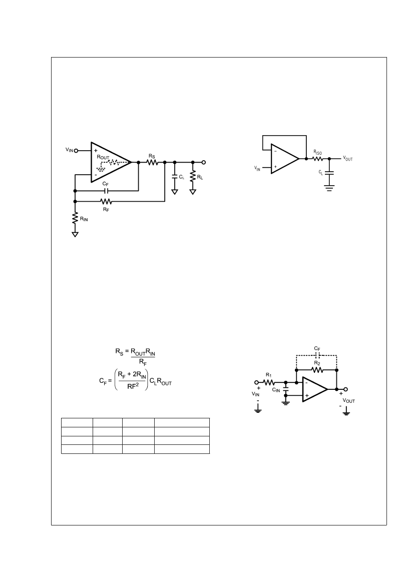
Application Notes
(Continued)
In the Loop Compensation
Figure 2
illustrates a compensation technique, known as ‘in
the loop’ compensation, that employs an RC feedback circuit
within the feedback loop to stabilize a non-inverting amplifier
configuration. A small series resistance, R
, is used to iso-
late the amplifier output from the load capacitance, C
L
, and a
small capacitance, C
F
, is inserted across the feedback re-
sistor to bypass C
L
at higher frequencies.
The values for R
and C
are decided by ensuring that the
zero attributed to C
lies at the same frequency as the pole
attributed to C
. This ensures that the effect of the second
pole on the transfer function is compensated for by the
presence of the zero, and that the ROC is maintained at
20 dB/decade. For the circuit shown in
Figure 2
the values of
R
and C
are given by
Equation (1)
.
Table 1
shows different
values of R
and C
that need to be used for maintaining
stability with different values of C
L
, as well as the phase
margins to be expected. R
and R
IN
are assumed to be 10
k
, R
L
is taken as 2 k
, while R
OUT
is taken to be 60
.
(1)
TABLE 1.
C
L
(pF)
250
300
500
R
S
(
)
60
60
60
C
F
(pF)
4.5
5.4
9
Phase Margin ()
39.8
49.5
53.1
Although this methodology provides circuit stability for any
load capacitance, it does so at the price of bandwidth. The
closed loop bandwidth of the circuit is now limited by R
S
and
C
F
.
Compensation by External Resistor
In some applications it is essential to drive a capacitive load
without sacrificing bandwidth. In such a case, in the loop
compensation is not viable. A simpler scheme for compen-
sation is shown in
Figure 3
. A resistor, R
, is placed in
series between the load capacitance and the output. This
introduces a zero in the circuit transfer function, which coun-
teracts the effect of the pole formed by the load capacitance,
and ensures stability.
The value of R
ISO
to be used should be decided depending
on the size of C
L
and the level of performance desired.
Values ranging from 5
to 50
are usually sufficient to
ensure stability. A larger value of R
ISO
will result in a system
with lesser ringing and overshoot, but will also limit the
output swing and the short circuit current of the circuit.
Stability and Input Capacitance
In certain applications, for example I-V conversion, transim-
pedance photodiode amplification and buffering the output of
current-output DAC, capacitive loading at the input of the op
amp can endanger stability. The capacitance of the source
driving the op amp, the op amp input capacitance and the
parasitic/wiring capacitance contribute to the loading of the
input. This capacitance, C
, interacts with the feedback
network to introduce a peaking in the closed loop gain of the
circuit, and hence causes instability.
This peaking can be eliminated by adding a feedback ca-
pacitance, C
F
, as shown in
Figure 4
. This introduces a zero
in the feedback network, and hence a pole in the closed loop
response, and thus maintains stability. An optimal value of
C
F
is given by
Equation (2)
. A simpler approach is to select
C
F
= (R
1
/R
2
)C
IN
for a 90 phase margin. This approach,
however, limits the bandwidth excessively.
20120338
FIGURE 2. In the Loop Compensation
20120356
FIGURE 3. Compensation By Isolation Resistor
20120349
FIGURE 4. Compensating for Input Capacitance
L
www.national.com
12
相關(guān)PDF資料 |
PDF描述 |
|---|---|
| LM6211MFX | Low Noise, RRO Operational Amplifier with CMOS Input and 24V Operation |
| LM62CIM3X | 2.7V, 15.6 mV/∑C SOT-23 Temperature Sensor |
| LM62BIM3 | 2.7V, 15.6 mV/∑C SOT-23 Temperature Sensor |
| LM62BIM3X | 2.7V, 15.6 mV/∑C SOT-23 Temperature Sensor |
| LM62CIM3 | 2.7V, 15.6 mV/∑C SOT-23 Temperature Sensor |
相關(guān)代理商/技術(shù)參數(shù) |
參數(shù)描述 |
|---|---|
| LM6211MF/NOPB | 功能描述:運(yùn)算放大器 - 運(yùn)放 Low Noise RRO Op Amp w/ CMOS Inpt 24V RoHS:否 制造商:STMicroelectronics 通道數(shù)量:4 共模抑制比(最小值):63 dB 輸入補(bǔ)償電壓:1 mV 輸入偏流(最大值):10 pA 工作電源電壓:2.7 V to 5.5 V 安裝風(fēng)格:SMD/SMT 封裝 / 箱體:QFN-16 轉(zhuǎn)換速度:0.89 V/us 關(guān)閉:No 輸出電流:55 mA 最大工作溫度:+ 125 C 封裝:Reel |
| LM6211MFX | 功能描述:運(yùn)算放大器 - 運(yùn)放 RoHS:否 制造商:STMicroelectronics 通道數(shù)量:4 共模抑制比(最小值):63 dB 輸入補(bǔ)償電壓:1 mV 輸入偏流(最大值):10 pA 工作電源電壓:2.7 V to 5.5 V 安裝風(fēng)格:SMD/SMT 封裝 / 箱體:QFN-16 轉(zhuǎn)換速度:0.89 V/us 關(guān)閉:No 輸出電流:55 mA 最大工作溫度:+ 125 C 封裝:Reel |
| LM6211MFX/NOPB | 功能描述:運(yùn)算放大器 - 運(yùn)放 RoHS:否 制造商:STMicroelectronics 通道數(shù)量:4 共模抑制比(最小值):63 dB 輸入補(bǔ)償電壓:1 mV 輸入偏流(最大值):10 pA 工作電源電壓:2.7 V to 5.5 V 安裝風(fēng)格:SMD/SMT 封裝 / 箱體:QFN-16 轉(zhuǎn)換速度:0.89 V/us 關(guān)閉:No 輸出電流:55 mA 最大工作溫度:+ 125 C 封裝:Reel |
| LM6218 | 制造商:未知廠家 制造商全稱:未知廠家 功能描述: |
| LM6218AH | 制造商:未知廠家 制造商全稱:未知廠家 功能描述:Voltage-Feedback Operational Amplifier |
發(fā)布緊急采購(gòu),3分鐘左右您將得到回復(fù)。