- 您現(xiàn)在的位置:買賣IC網(wǎng) > PDF目錄30753 > LM4854MTX/NOPB (NATIONAL SEMICONDUCTOR CORP) 0.2 W, 2 CHANNEL, AUDIO AMPLIFIER, PDSO14 PDF資料下載
參數(shù)資料
| 型號: | LM4854MTX/NOPB |
| 廠商: | NATIONAL SEMICONDUCTOR CORP |
| 元件分類: | 音頻/視頻放大 |
| 英文描述: | 0.2 W, 2 CHANNEL, AUDIO AMPLIFIER, PDSO14 |
| 封裝: | TSSOP-14 |
| 文件頁數(shù): | 16/29頁 |
| 文件大?。?/td> | 1440K |
| 代理商: | LM4854MTX/NOPB |
第1頁第2頁第3頁第4頁第5頁第6頁第7頁第8頁第9頁第10頁第11頁第12頁第13頁第14頁第15頁當前第16頁第17頁第18頁第19頁第20頁第21頁第22頁第23頁第24頁第25頁第26頁第27頁第28頁第29頁

Application Information (Continued)
OPTIMIZING CLICK AND POP REDUCTION PERFOR-
MANCE
The LM4854 contains circuitry that eliminates turn-on and
shutdown transients ("clicks and pops") and transients that
could occur when switching between BTL speakers and
single-ended headphones. For this discussion, turn-on re-
fers to either applying the power supply voltage or when the
micro-power shutdown mode is deactivated.
As the V
DD/2 voltage present at the BYPASS pin ramps to its
final value, the LM4854’s internal amplifiers are configured
as unity gain buffers and are disconnected from the L-OUT,
BTL-OUT, and R-OUT pins. An internal current source
charges the capacitor connected between the BYPASS pin
and GND in a controlled, linear manner. Ideally, the input and
outputs track the voltage applied to the BYPASS pin. The
gain of the internal amplifiers remains unity until the voltage
on the bypass pin reaches V
DD/2. Once the voltage on the
bypass pin is stable and after a fixed nominal delay of
120ms, the device becomes fully operational and the ampli-
fier outputs are reconnected to their respective output pins.
Although the BYPASS pin current cannot be modified,
changing the size of CB alters the device’s turn-on time.
There is a linear relationship between the size of CB and the
turn-on time. Here are some typical turn-on times for various
values of CB:
C
B (F)
T
ON (ms)
0.01
120
0.1
130
0.22
140
0.47
160
1.0
200
2.2
300
In order eliminate "clicks and pops", all capacitors must be
discharged before turn-on. Rapidly switching V
DD may not
allow the capacitors to fully discharge, which may cause
"clicks and pops".
AUDIO POWER AMPLIFIER DESIGN
Audio Amplifier Design: Driving 1W into an 8
Load
The following are the desired operational parameters:
Power Output:
1W
RMS
Load Impedance
8
Input Level:
1V
RMS
Input Impedance:
20k
Bandwidth:
100Hz - 20kHz ± 0.25dB
The design begins by specifying the minimum supply voltage
necessary to obtain the specified output power. One way to
find the minimum supply voltage is to use the Output Power
vs Supply Voltage curve in the Typical Performance Charac-
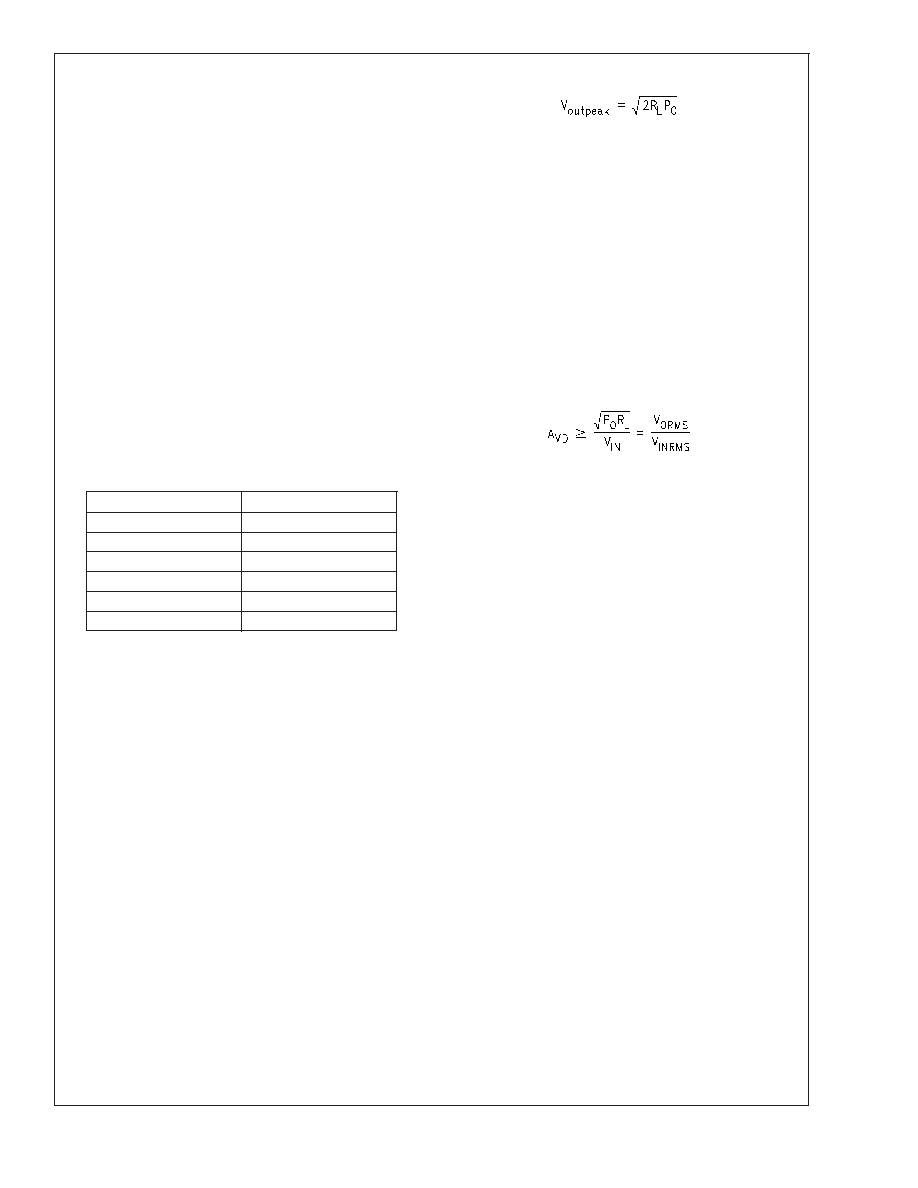
teristics section. Another way, using Equation (8), is to cal-
culate the peak output voltage necessary to achieve the
desired output power for a given load impedance. To ac-
count for the amplifier’s dropout voltage, two additional volt-
ages, based on the Dropout Voltage vs Supply Voltage in the
Typical Performance Characteristics curves, must be added
to the result obtained by Equation (8). The result is Equation
(9).
(8)
V
DD =VOUTPEAK +VODTOP +VODBOT
(9)
The Output Power vs. Supply Voltage graph for an 8
load
indicates a minimum supply voltage of 4.6V. The commonly
used 5V supply voltage easily meets this. The additional
voltage creates the benefit of headroom, allowing the
LM4854 to produce peak output power in excess of 1W
without clipping or other audible distortion. The choice of
supply voltage must also not create a situation that violates
of maximum power dissipation as explained above in the
Power Dissipation section. After satisfying the LM4854’s
power dissipation requirements, the minimum differential
gain needed to achieve 1W dissipation in an 8
load is
found using Equation (10).
(10)
Thus, a minimum gain of 2.83 allows the LM4854’s to reach
full output swing and maintain low noise and THD+N perfor-
mance. For this example, let AVD = 3. The amplifier’s overall
gain is set using the input (R
i) and feedback (Rf) resistors.
With the desired input impedance set at 20k
, the feedback
resistor is found using Equation (11).
R
f /Ri =AVD / 2
(11)
The value of R
f is 30k
. The nominal output power is 1.13W.
TThe last step in this design example is setting the amplifi-
er’s -3dB frequency bandwidth. To achieve the desired
±0.25dB pass band magnitude variation limit, the low fre-
quency response must extend to at least one-fifth the lower
bandwidth limit and the high frequency response must ex-
tend to at least five times the upper bandwidth limit. The gain
variation for both response limits is 0.17dB, well within the
±0.25dB-desired limit. The results are an
f
L = 100Hz / 5 = 20Hz
(12)
and an
f
L = 20kHz x 5 = 100kHz
(13)
As mentioned in the SELECTING EXTERNAL COMPO-
NENTS section, R
i and Ci create a highpass filter that sets
the amplifier’s lower bandpass frequency limit. Find the cou-
pling capacitor’s value using Equation (14).
C
i =1/(2
πR
ifL)
(14)
The result is
1/(2
π x 20k x 20Hz) = 0.397F
(15)
Use a 0.39F capacitor, the closest standard value.
LM4854
www.national.com
23
相關(guān)PDF資料 |
PDF描述 |
|---|---|
| LM4854LD/NOPB | 0.2 W, 2 CHANNEL, AUDIO AMPLIFIER, PDSO14 |
| LM4854LDX/NOPB | 0.2 W, 2 CHANNEL, AUDIO AMPLIFIER, PDSO14 |
| LM4856LQ/NOPB | 1.5 W, 3 CHANNEL, AUDIO AMPLIFIER, QCC24 |
| LM4856ITL/NOPB | 1.1 W, 3 CHANNEL, AUDIO AMPLIFIER, PBGA18 |
| LM4857GR/NOPB | SPECIALTY CONSUMER CIRCUIT, PBGA49 |
相關(guān)代理商/技術(shù)參數(shù) |
參數(shù)描述 |
|---|---|
| LM4855 | 制造商:NSC 制造商全稱:National Semiconductor 功能描述:Boomer AUDIO POWER AMPLIFIER Integrated Audio Amplifier System |
| LM48555 | 制造商:NSC 制造商全稱:National Semiconductor 功能描述:Ceramic Speaker Driver |
| LM48555TL | 制造商:Texas Instruments 功能描述:Audio Amp Speaker 1-CH Mono Class-AB 12-Pin uSMD T/R 制造商:Texas Instruments 功能描述:IC AMP POWER AUDIO SMD |
| LM48555TL/NOPB | 功能描述:音頻放大器 RoHS:否 制造商:STMicroelectronics 產(chǎn)品:General Purpose Audio Amplifiers 輸出類型:Digital 輸出功率: THD + 噪聲: 工作電源電壓:3.3 V 電源電流: 最大功率耗散: 最大工作溫度: 安裝風格:SMD/SMT 封裝 / 箱體:TQFP-64 封裝:Reel |
| LM48555TLBD | 功能描述:音頻 IC 開發(fā)工具 LM48555TL EVAL BOARD RoHS:否 制造商:Texas Instruments 產(chǎn)品:Evaluation Kits 類型:Audio Amplifiers 工具用于評估:TAS5614L 工作電源電壓:12 V to 38 V |
發(fā)布緊急采購,3分鐘左右您將得到回復(fù)。