- 您現(xiàn)在的位置:買賣IC網(wǎng) > PDF目錄30753 > LM4850MTX/NOPB (NATIONAL SEMICONDUCTOR CORP) 0.3 W, 2 CHANNEL, AUDIO AMPLIFIER, PDSO14 PDF資料下載
參數(shù)資料
| 型號(hào): | LM4850MTX/NOPB |
| 廠商: | NATIONAL SEMICONDUCTOR CORP |
| 元件分類: | 音頻/視頻放大 |
| 英文描述: | 0.3 W, 2 CHANNEL, AUDIO AMPLIFIER, PDSO14 |
| 封裝: | 4.40 MM, PLASTIC, TSSOP-14 |
| 文件頁數(shù): | 13/18頁 |
| 文件大小: | 1273K |
| 代理商: | LM4850MTX/NOPB |
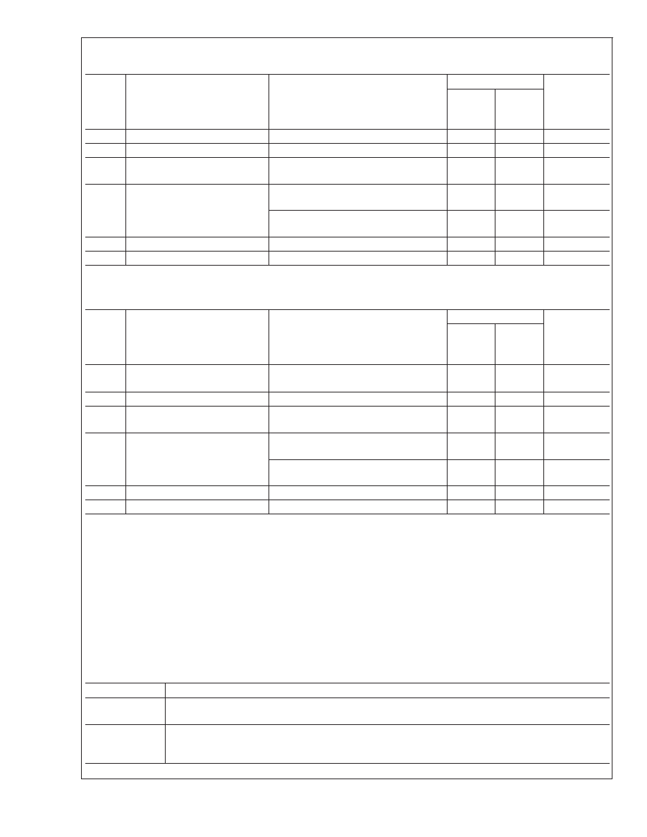
Electrical Characteristics (Notes 3, 9) (Continued)
The following specifications apply for V
DD= 3.3V, TA= 25C unless otherwise specified.
Symbol
Parameter
Conditions
LM4850
Units
(Limits)
Typical
Limit
SE Mode; V
IN = 0V; IO = 0A
2.0
mA
I
SD
Shutdown Current
SD Mode
30
A
V
OS
Output Offset Voltage
BTL Mode; A
V =2
BTL OUT+ to BTL OUT
5.0
40
mV
P
O
Output Power
BTL Mode; R
L =8
THD+N = 1%
440
mW
SE Mode; R
L =32
THD+N = 1%
40
mW
V
IH
Shutdown Input Voltage High
Is < 80A
2.0
V (min)
V
IL
Shutdown Input Voltage Low
Is > 0.5mA
0.8
V (max)
Electrical Characteristics(Notes 3, 9)
The following specifications apply for V
DD= 2.7V, TA= 25C unless otherwise specified.
Symbol
Parameter
Conditions
LM4850
Units
(Limits)
Typical
Limit
I
DD
Supply Current
BTL Mode; V
IN = 0V; IO = 0A
1.8
mA
SE Mode; V
IN = 0V; IO = 0A
1.8
mA
I
SD
Shutdown Current
SD Mode
25
A
V
OS
Output Offset Voltage
BTL Mode; A
V =2
BTL OUT+ to BTL OUT
5.0
40
mV
P
O
Output Power
BTL Mode; R
L =8
THD+N = 1%
300
mW
SE Mode; R
L =32
THD+N = 1%
25
mW
V
IH
Shutdown Input Voltage High
Is < 80 A
2.0
V (min)
V
IL
Shutdown Input Voltage Low
Is > 0.5mA
0.8
V (max)
Note 3: Absolute Maximum Rating indicate limits beyond which damage to
the device may occur.
Note 4: Operating Ratings indicate conditions for which the device is func-
tional, but do not guarantee specific performance limits. For guaranteed
specifications and test conditions, see the Electrical Characteristics. The
guaranteed specifications apply only for the test conditions listed. Some
performance characteristics may degrade when the device is not operated
under the listed test conditions.
Note 5: Human body model, 100pF discharged through a 1.5k
resistor.
Note 6: Typical specifications are specified at +25C and represent the most
likely parametric norm.
Note 7: Datasheet min/max specification limits are guaranteed by design,
test, or statistical analysis.
Note 8: Machine Model ESD test is covered by specification EIAJ
IC-121-1981. A 200pF cap is charged to the specified voltage, then dis-
charged directly into the IC with no external series resistor (resistance of
discharge path must be under 50
).
Note 9: All voltages are measured with respect to the ground pin, unless
otherwise specified.
Note 10: The given
θJA is for a LM4850LD with the Exposed-DAP soldered
to an exposed 1in2 area of 1oz printed circuit board copper.
Note 11: When driving 3
or 4 loads from a 5V supply, the LM4850 must
be mounted to a circuit board.
Note 12: Limits are guaranteed to National’s AOQL ( Average Outgoing
Quality Level ).
External Components Description
(Refer to Figure 1.)
Components
Functional Description
1.
R
i
Inverting input resistance which sets the closed-loop gain in conjunction with R
f. This resistor also forms a
high pass filter with C
i at fc = 1/(2πRiCi).
2.
C
i
Input coupling capacitor which blocks the DC voltage at the amplifier’s input terminals. Also creates a
highpass filter with R
i at fc = 1/(2πRiCi). Refer to the section, Proper Selection of External Components,
for an explanation of how to determine the value of C
i.
LM4850
www.national.com
4
相關(guān)PDF資料 |
PDF描述 |
|---|---|
| LM4851ITL/NOPB | 1.1 W, 3 CHANNEL, AUDIO AMPLIFIER, PBGA18 |
| LM4851LQ/NOPB | 1.5 W, 3 CHANNEL, AUDIO AMPLIFIER, QCC24 |
| LM4852LQ/NOPB | 1.5 W, 3 CHANNEL, AUDIO AMPLIFIER, QCC24 |
| LM4852ITL/NOPB | 1.1 W, 3 CHANNEL, AUDIO AMPLIFIER, PBGA18 |
| LM4854MT/NOPB | 0.2 W, 2 CHANNEL, AUDIO AMPLIFIER, PDSO14 |
相關(guān)代理商/技術(shù)參數(shù) |
參數(shù)描述 |
|---|---|
| LM4851 | 制造商:NSC 制造商全稱:National Semiconductor 功能描述:Integrated Audio Amplifier System |
| LM48510 | 制造商:NSC 制造商全稱:National Semiconductor 功能描述:Boosted Class D Audio Power Amplifier |
| LM48510_0710 | 制造商:NSC 制造商全稱:National Semiconductor 功能描述:Boosted Class D Audio Power Amplifier |
| LM48510SD | 功能描述:音頻放大器 RoHS:否 制造商:STMicroelectronics 產(chǎn)品:General Purpose Audio Amplifiers 輸出類型:Digital 輸出功率: THD + 噪聲: 工作電源電壓:3.3 V 電源電流: 最大功率耗散: 最大工作溫度: 安裝風(fēng)格:SMD/SMT 封裝 / 箱體:TQFP-64 封裝:Reel |
| LM48510SD/NOPB | 功能描述:音頻放大器 RoHS:否 制造商:STMicroelectronics 產(chǎn)品:General Purpose Audio Amplifiers 輸出類型:Digital 輸出功率: THD + 噪聲: 工作電源電壓:3.3 V 電源電流: 最大功率耗散: 最大工作溫度: 安裝風(fēng)格:SMD/SMT 封裝 / 箱體:TQFP-64 封裝:Reel |
發(fā)布緊急采購,3分鐘左右您將得到回復(fù)。