- 您現(xiàn)在的位置:買賣IC網(wǎng) > PDF目錄385481 > LM3478MMX (NATIONAL SEMICONDUCTOR CORP) High Efficiency Low-Side N-Channel Controller for Switching Regulator PDF資料下載
參數(shù)資料
| 型號: | LM3478MMX |
| 廠商: | NATIONAL SEMICONDUCTOR CORP |
| 元件分類: | 穩(wěn)壓器 |
| 英文描述: | High Efficiency Low-Side N-Channel Controller for Switching Regulator |
| 中文描述: | 1 A SWITCHING CONTROLLER, 1000 kHz SWITCHING FREQ-MAX, PDSO8 |
| 封裝: | MSOP-8 |
| 文件頁數(shù): | 17/21頁 |
| 文件大小: | 624K |
| 代理商: | LM3478MMX |
Typical Applications
(Continued)
where D
MAX
is the maximum duty cycle.
The turn-on and turn-off transitions of a MOSFET require
times of tens of nano-seconds. C
and Q
are needed to
estimate the large instantaneous power loss that occurs
during these transitions.
The amount of gate current required to turn the MOSFET on
can be calculated using the formula:
I
G
= Q
g
.F
S
The required gate drive power to turn the MOSFET on is
equal to the switching frequency times the energy required
to deliver the charge to bring the gate charge voltage to V
DR
(see electrical characteristics and typical performance char-
acteristics for the drive voltage specification).
P
Drive
= F
S
.Q
g
.V
DR
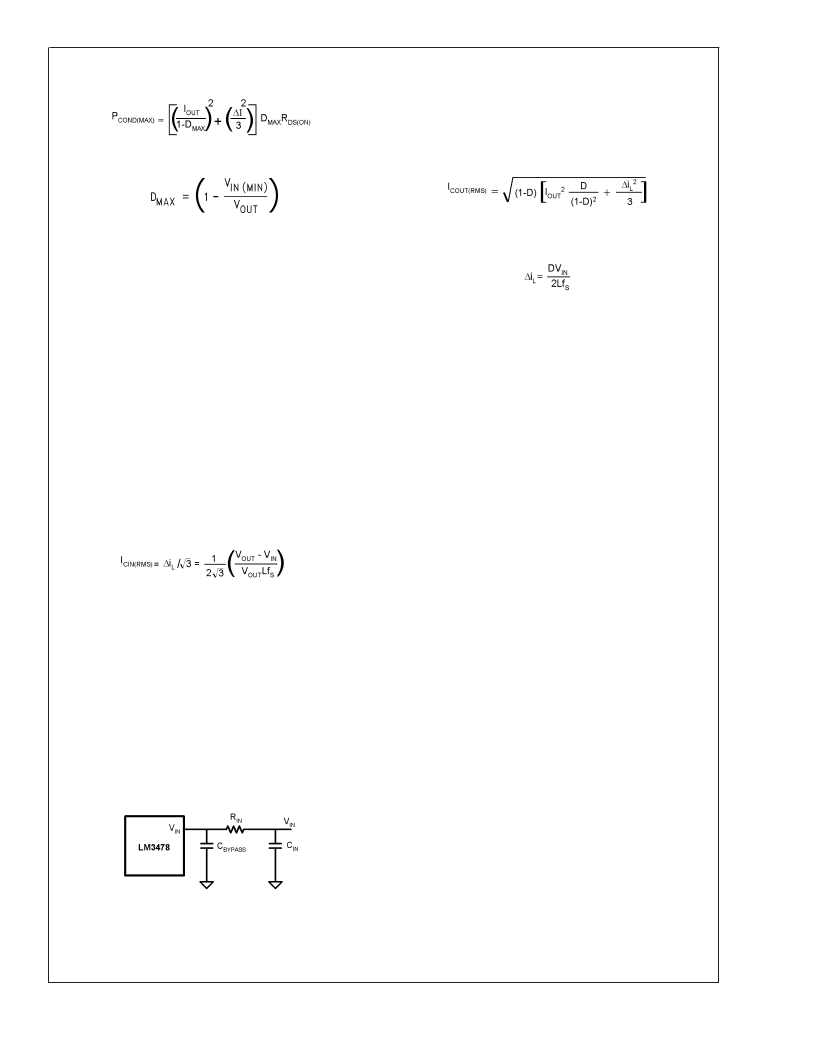
INPUT CAPACITOR SELECTION
Due to the presence of an inductor at the input of a boost
converter, the input current waveform is continuous and
triangular, as shown in
Figure 9
. The inductor ensures that
the input capacitor sees fairly low ripple currents. However,
as the input capacitor gets smaller, the input ripple goes up.
The rms current in the input capacitor is given by:
The input capacitor should be capable of handling the rms
current. Although the input capacitor is not as critical in a
boost application, low values can cause impedance interac-
tions. Therefore a good quality capacitor should be chosen
in the range of 100μF to 200μF. If a value lower than 100μF
is used than problems with impedance interactions or
switching noise can affect the LM3478. To improve perfor-
mance, especially with V
IN
below 8 volts, it is recommended
to use a 20
resistor at the input to provide a RC filter. The
resistor is placed in series with the V
IN
pin with only a bypass
capacitor attached to the V
pin directly (see
Figure 11
). A
0.1μF or 1μF ceramic capacitor is necessary in this configu-
ration. The bulk input capacitor and inductor will connect on
the other side of the resistor with the input power supply.
OUTPUT CAPACITOR SELECTION
The output capacitor in a boost converter provides all the
output current when the inductor is charging. As a result it
sees very large ripple currents. The output capacitor should
be capable of handling the maximum rms current. The rms
current in the output capacitor is:
Where
and D, the duty cycle is equal to (V
OUT
V
IN
)/V
OUT
.
The ESR and ESL of the output capacitor directly control the
output ripple. Use capacitors with low ESR and ESL at the
output for high efficiency and low ripple voltage. Surface
Mount tantalums, surface mount polymer electrolytic and
polymer tantalum, Sanyo- OSCON, or multi-layer ceramic
capacitors are recommended at the output.
Designing SEPIC Using LM3478
Since the LM3478 controls a low-side N-Channel MOSFET,
it can also be used in SEPIC (Single Ended Primary Induc-
tance Converter) applications. An example of SEPIC using
LM3478 is shown in
Figure 12
. As shown in
Figure 12
, the
output voltage can be higher or lower than the input voltage.
The SEPIC uses two inductors to step-up or step-down the
input voltage. The inductors L1 and L2 can be two discrete
inductors or two windings of a coupled transformer since
equal voltages are applied across the inductor throughout
the switching cycle. Using two discrete inductors allows use
of catalog magnetics, as opposed to a custom transformer.
The input ripple can be reduced along with size by using the
coupled windings of transformer for L1 and L2.
Due to the presence of the inductor L1 at the input, the
SEPIC inherits all the benefits of a boost converter. One
main advantage of SEPIC over boost converter is the inher-
ent input to output isolation. The capacitor CS isolates the
input from the output and provides protection against
shorted or malfunctioning load. Hence, theASEPIC is useful
for replacing boost circuits when true shutdown is required.
This means that the output voltage falls to 0V when the
switch is turned off. In a boost converter, the output can only
fall to the input voltage minus a diode drop.
10135593
FIGURE 11. Reducing IC Input Noise
L
www.national.com
17
相關(guān)PDF資料 |
PDF描述 |
|---|---|
| LM3485 | Hysteretic PFET Buck Controller |
| LM3485MM | Hysteretic PFET Buck Controller |
| LM3485MMX | Hysteretic PFET Buck Controller |
| LM3488 | 500kHz and 1MHz High Efficiency 1.5A Switching Regulators; Package: SO; No of Pins: 8; Temperature Range: -40?°C to 85?°C |
| LM3488MM | 500kHz and 1MHz High Efficiency 1.5A Switching Regulators; Package: SO; No of Pins: 8; Temperature Range: -40?°C to 85?°C |
相關(guān)代理商/技術(shù)參數(shù) |
參數(shù)描述 |
|---|---|
| LM3478MMX/HALF | 制造商:Texas Instruments 功能描述: |
| LM3478MMX/NOPB | 功能描述:DC/DC 開關(guān)控制器 RoHS:否 制造商:Texas Instruments 輸入電壓:6 V to 100 V 開關(guān)頻率: 輸出電壓:1.215 V to 80 V 輸出電流:3.5 A 輸出端數(shù)量:1 最大工作溫度:+ 125 C 安裝風(fēng)格: 封裝 / 箱體:CPAK |
| LM3478MMX/S5000472 | 制造商:Texas Instruments 功能描述: |
| LM3478Q | 制造商:NSC 制造商全稱:National Semiconductor 功能描述:High Efficiency Low-Side N-Channel Controller for Switching Regulator |
| LM3478QMM | 制造商:NSC 制造商全稱:National Semiconductor 功能描述:High Efficiency Low-Side N-Channel Controller for Switching Regulator |
發(fā)布緊急采購,3分鐘左右您將得到回復(fù)。