- 您現(xiàn)在的位置:買(mǎi)賣(mài)IC網(wǎng) > PDF目錄385480 > LM3310SQX (NATIONAL SEMICONDUCTOR CORP) Step-up PWM DC/DC Converter with Integrated Op-Amp and Gate Pulse Modulation Switch PDF資料下載
參數(shù)資料
| 型號(hào): | LM3310SQX |
| 廠(chǎng)商: | NATIONAL SEMICONDUCTOR CORP |
| 元件分類(lèi): | 穩(wěn)壓器 |
| 英文描述: | Step-up PWM DC/DC Converter with Integrated Op-Amp and Gate Pulse Modulation Switch |
| 中文描述: | 2.6 A SWITCHING REGULATOR, 1500 kHz SWITCHING FREQ-MAX, QCC24 |
| 封裝: | LLP-24 |
| 文件頁(yè)數(shù): | 19/25頁(yè) |
| 文件大?。?/td> | 1668K |
| 代理商: | LM3310SQX |
第1頁(yè)第2頁(yè)第3頁(yè)第4頁(yè)第5頁(yè)第6頁(yè)第7頁(yè)第8頁(yè)第9頁(yè)第10頁(yè)第11頁(yè)第12頁(yè)第13頁(yè)第14頁(yè)第15頁(yè)第16頁(yè)第17頁(yè)第18頁(yè)當(dāng)前第19頁(yè)第20頁(yè)第21頁(yè)第22頁(yè)第23頁(yè)第24頁(yè)第25頁(yè)
Operation
(Continued)
Now R
can be chosen with the selected value for C
C
.
Check to make sure that the pole f
is still in the 10Hz to
500Hz range, change each value slightly if needed to ensure
both component values are in the recommended range.
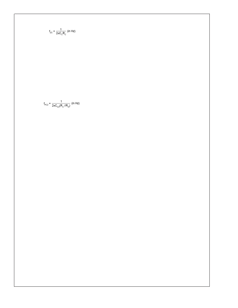
HIGH OUTPUT CAPACITOR ESR COMPENSATION
When using an output capacitor with a high ESR value, or
just to improve the overall phase margin of the control loop,
another pole may be introduced to cancel the zero created
by the ESR. This is accomplished by adding another capaci-
tor, C
C2
, directly from the compensation pin V
C
to ground, in
parallel with the series combination of R
C
and C
C
. The pole
should be placed at the same frequency as f
Z1
, the ESR
zero. The equation for this pole follows:
To ensure this equation is valid, and that C
C2
can be used
without negatively impacting the effects of R
C
and C
C
, f
PC2
must be greater than 10f
ZC
.
CHECKING THE DESIGN
With all the poles and zeros calculated the crossover fre-
quency can be checked as described in the section
DC Gain
and Open-loop Gain
. The compensation values can be
changed a little more to optimize performance if desired.
This is best done in the lab on a bench, checking the load
step response with different values until the ringing and
overshoot on the output voltage at the edge of the load steps
is minimal. This should produce a stable, high performance
circuit. For improved transient response, higher values of R
C
should be chosen. This will improve the overall bandwidth
which makes the regulator respond more quickly to tran-
sients. If more detail is required, or the most optimum per-
formance is desired, refer to a more in depth discussion of
compensating current mode DC/DC switching regulators.
POWER DISSIPATION
The output power of the LM3310 is limited by its maximum
power dissipation. The maximum power dissipation is deter-
mined by the formula
P
D
= (T
jmax
- T
A
)/
θ
JA
where T
jmax
is the maximum specified junction temperature
(125C), T
A
is the ambient temperature, and
θ
JA
is the ther-
mal resistance of the package.
LAYOUT CONSIDERATIONS
The input bypass capacitor C
, as shown in the typical
operating circuit, must be placed close to the IC. This will
reduce copper trace resistance which effects input voltage
ripple of the IC. For additional input voltage filtering, a 100nF
bypass capacitor can be placed in parallel with C
, close to
the V
pin, to shunt any high frequency noise to ground. The
output capacitor, C
, should also be placed close to the
IC. Any copper trace connections for the C
capacitor can
increase the series resistance, which directly effects output
voltage ripple. The feedback network, resistors R
and
R
, should be kept close to the FB pin, and away from the
inductor, to minimize copper trace connections that can in-
ject noise into the system. R
and C
should also be close to
the RE and CE pins to minimize noise in the GPM circuitry.
Trace connections made to the inductor and schottky diode
should be minimized to reduce power dissipation and in-
crease overall efficiency. For more detail on switching power
supply layout considerations see Application Note AN-1149:
Layout Guidelines for Switching Power Supplies
.
For Op-Amp layout please refer to the
Operational Amplifier
section.
Figure 6
,
Figure 7
, and
Figure 8
in the Application Informa-
tion section following show the schematic and an example of
a good layout as used in the LM3310/11 evaluation board.
L
www.national.com
19
相關(guān)PDF資料 |
PDF描述 |
|---|---|
| LM3351 | Switched Capacitor Voltage Converter |
| LM3351MM | Switched Capacitor Voltage Converter |
| LM3351MMX | Switched Capacitor Voltage Converter |
| LM3355MM-4.1 | Regulated 50mA Buck-Boost Switched Capacitor DC/DC Converter |
| LM3355MMX-4.1 | Regulated 50mA Buck-Boost Switched Capacitor DC/DC Converter |
相關(guān)代理商/技術(shù)參數(shù) |
參數(shù)描述 |
|---|---|
| LM3310SQX/NOPB | 功能描述:DC/DC 開(kāi)關(guān)控制器 RoHS:否 制造商:Texas Instruments 輸入電壓:6 V to 100 V 開(kāi)關(guān)頻率: 輸出電壓:1.215 V to 80 V 輸出電流:3.5 A 輸出端數(shù)量:1 最大工作溫度:+ 125 C 安裝風(fēng)格: 封裝 / 箱體:CPAK |
| LM3311 | 制造商:NSC 制造商全稱(chēng):National Semiconductor 功能描述:Step-Up PWM DC/DC Converter with Integrated LDO, Op-Amp, and Gate Pulse Modulation Switch |
| LM3311_07 | 制造商:NSC 制造商全稱(chēng):National Semiconductor 功能描述:Step-Up PWM DC/DC Converter with Integrated LDO, Op-Amp, and Gate Pulse Modulation Switch |
| LM3311SQ | 制造商:Texas Instruments 功能描述:CONVERTER DC/DC STEP UP LLP-24 |
| LM3311SQ/NOPB | 功能描述:IC REG BOOST ADJ 2A DL 24LLP RoHS:是 類(lèi)別:集成電路 (IC) >> PMIC - 穩(wěn)壓器 - DC DC 開(kāi)關(guān)穩(wěn)壓器 系列:- 產(chǎn)品培訓(xùn)模塊:Lead (SnPb) Finish for COTS Obsolescence Mitigation Program 標(biāo)準(zhǔn)包裝:1 系列:- 類(lèi)型:降壓(降壓) 輸出類(lèi)型:固定 輸出數(shù):1 輸出電壓:3.3V 輸入電壓:4.5 V ~ 24 V PWM 型:- 頻率 - 開(kāi)關(guān):- 電流 - 輸出:125mA 同步整流器:無(wú) 工作溫度:-40°C ~ 85°C 安裝類(lèi)型:表面貼裝 封裝/外殼:SOT-23-6 包裝:Digi-Reel® 供應(yīng)商設(shè)備封裝:SOT-6 其它名稱(chēng):MAX1836EUT33#TG16DKR |
發(fā)布緊急采購(gòu),3分鐘左右您將得到回復(fù)。