- 您現(xiàn)在的位置:買賣IC網(wǎng) > PDF目錄385480 > LM3100MH (NATIONAL SEMICONDUCTOR CORP) SIMPLE SWITCHER㈢ Synchronous 1MHz 1.5A Step-Down Voltage Regulator PDF資料下載
參數(shù)資料
| 型號: | LM3100MH |
| 廠商: | NATIONAL SEMICONDUCTOR CORP |
| 元件分類: | 穩(wěn)壓器 |
| 英文描述: | SIMPLE SWITCHER㈢ Synchronous 1MHz 1.5A Step-Down Voltage Regulator |
| 中文描述: | 1.9 A SWITCHING REGULATOR, 1000 kHz SWITCHING FREQ-MAX, PDSO20 |
| 封裝: | PLASTIC, TSSOP-20 |
| 文件頁數(shù): | 13/15頁 |
| 文件大小: | 1073K |
| 代理商: | LM3100MH |
Applications Information
(Continued)
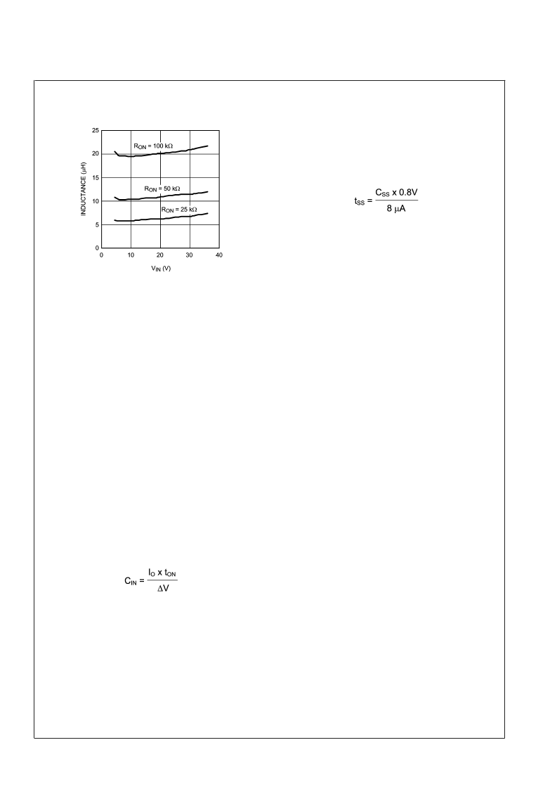
Inductor Selector for V
OUT
= 0.8V
20174737
C
VCC
:
The capacitor on the V
output provides not only
noise filtering and stability, but also prevents false triggering
of the V
UVLO at the buck switch on/off transitions. For
this reason, C
should be no smaller than 680 nF for
stability, and should be a good quality, low ESR, ceramic
capacitor.
C
O
and C
O3
:
C
O
should generally be no smaller than 10 μF.
Experimentation is usually necessary to determine the mini-
mum value for C
O
, as the nature of the load may require a
larger value. A load which creates significant transients re-
quires a larger value for C
O
than a fixed load.
C
O3
is a small value ceramic capacitor to further suppress
high frequency noise at V
OUT
. A 47nF is recommended,
located close to the LM3100.
C
and C
:
C
’s purpose is to supply most of the switch
current during the on-time, and limit the voltage ripple at V
,
on the assumption that the voltage source feeding V
has
an output impedance greater than zero. If the source’s dy-
namic impedance is high (effectively a current source), it
supplies the average input current, but not the ripple current.
At maximum load current, when the buck switch turns on, the
current into V
suddenly increases to the lower peak of the
inductor’s ripple current, ramps up to the peak value, then
drop to zero at turn-off. The average current during the
on-time is the load current. For a worst case calculation, C
IN
must supply this average load current during the maximum
on-time. C
IN
is calculated from:
(8)
where I
is the load current, t
is the maximum on-time,
and
V is the allowable ripple voltage at V
IN
.
C
’s purpose is to help avoid transients and ringing due to
long lead inductance at V
. A low ESR, 0.1μF ceramic chip
capacitor is recommended, located close to the LM3100.
C
:
The recommended value for CBST is 33 nF. A high
quality ceramic capacitor with low ESR is recommended as
C
supplies a surge current to charge the buck switch gate
at turn-on.Alow ESR also helps ensure a complete recharge
during each off-time.
C
:
The capacitor at the SS pin determines the soft-start
time, i.e. the time for the reference voltage at the regulation
comparator, and the output voltage, to reach their final value.
The time is determined from the following:
C
:
If output voltage is higher than 1.6V, this feedback cap
is needed for Discontinuous Conduction Mode to improve
the output ripple performance, the recommended value for
C
FB
is 10 nF.
PC BOARD LAYOUT
The LM3100 regulation, over-voltage, and current limit com-
parators are very fast, and will respond to short duration
noise pulses. Layout considerations are therefore critical for
optimum performance. The layout must be as neat and
compact as possible, and all of the components must be as
close as possible to their associated pins. Refer to the
functional block diagram, the loop formed by C
, the high
and low-side switches internal to the IC, and the PGND pin
should be as small as possible. The PGND connection to Cin
should be as short and direct as possible. There should be
several vias connecting the Cin ground terminal to the
ground plane placed as close to the capacitor as possible.
The boost capacitor should be connected as close to the SW
and BST pins as possible. The feedback divider resistors
and the C
FB
capacitor should be located close to the FB pin.
A long trace run from the top of the divider to the output is
generally acceptable since this is a low impedance node.
Ground the bottom of the divider directly to the GND (pin 7).
The output capacitor, C
OUT
, should be connected close to
the load and tied directly into the ground plane. The inductor
should connect close to the SW pin with as short a trace as
possible to help reduce the potential for EMI (electro-
magnetic interference) generation.
If it is expected that the internal dissipation of the LM3100
will produce excessive junction temperatures during normal
operation, good use of the PC board’s ground plane can help
considerably to dissipate heat. The exposed pad on the
bottom of the IC package can be soldered to a ground plane
and that plane should extend out from beneath the IC to help
dissipate the heat. The exposed pad is internally connected
to the IC substrate. Additionally the use of wide PC board
traces, where possible, can help conduct heat away from the
IC. Using numerous vias to connect the die attach pad to an
internal ground plane is a good practice. Judicious position-
ing of the PC board within the end product, along with the
use of any available air flow (forced or natural convection)
can help reduce the junction temperature.
L
www.national.com
13
相關(guān)PDF資料 |
PDF描述 |
|---|---|
| LM3100MHX | SIMPLE SWITCHER㈢ Synchronous 1MHz 1.5A Step-Down Voltage Regulator |
| LM3189 | LM3189 FM IF System |
| LM3189N | LM3189 FM IF System |
| LM3202 | 650mA Miniature, Adjustable, Step-Down DC-DC Converter for RF Power Amplifiers |
| LM3202TL | 650mA Miniature, Adjustable, Step-Down DC-DC Converter for RF Power Amplifiers |
相關(guān)代理商/技術(shù)參數(shù) |
參數(shù)描述 |
|---|---|
| LM3100MH/NOPB | 功能描述:直流/直流開關(guān)轉(zhuǎn)換器 SYNC 1MHZ 1.5A STEP- DOWN VLTG REG RoHS:否 制造商:STMicroelectronics 最大輸入電壓:4.5 V 開關(guān)頻率:1.5 MHz 輸出電壓:4.6 V 輸出電流:250 mA 輸出端數(shù)量:2 最大工作溫度:+ 85 C 安裝風(fēng)格:SMD/SMT |
| LM3100MHX | 功能描述:直流/直流開關(guān)轉(zhuǎn)換器 RoHS:否 制造商:STMicroelectronics 最大輸入電壓:4.5 V 開關(guān)頻率:1.5 MHz 輸出電壓:4.6 V 輸出電流:250 mA 輸出端數(shù)量:2 最大工作溫度:+ 85 C 安裝風(fēng)格:SMD/SMT |
| LM3100MHX/NOPB | 功能描述:直流/直流開關(guān)轉(zhuǎn)換器 RoHS:否 制造商:STMicroelectronics 最大輸入電壓:4.5 V 開關(guān)頻率:1.5 MHz 輸出電壓:4.6 V 輸出電流:250 mA 輸出端數(shù)量:2 最大工作溫度:+ 85 C 安裝風(fēng)格:SMD/SMT |
| LM3101 | 制造商:NSC 制造商全稱:National Semiconductor 功能描述:Secondary-Side PWM Controller |
| LM3101M | 制造商:NSC 制造商全稱:National Semiconductor 功能描述:Secondary-Side PWM Controller |
發(fā)布緊急采購,3分鐘左右您將得到回復(fù)。