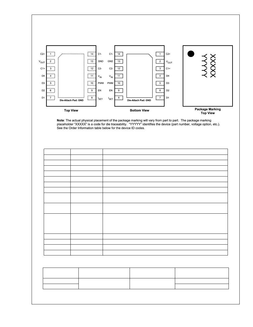
Connection Diagram
LM27952
14-pin No-Pullback Leadless Leadframe Package (LLP-14)
4mm x 3mm x 0.8mm
NS Package Number SDA14A
20148002
Pin Description
Pin
1
2
3
4
5
6
7
8
Name
C2+
V
OUT
C1+
D4
D3
D2
D1
I
SET
Description
Flying Capacitor C2 Connection
Pre-Regulated Charge Pump Output
Flying Capacitor C1 Connection
Regulated Current Sink Input.
Regulated Current Sink Input.
Regulated Current Sink Input.
Regulated Current Sink Input.
Current Set Input. Placing a resistor (R
SET
) between this pin and GND sets
the LED current for all the LEDs. LED Current = 200 x (1.25V ÷ R
SET
).
Enable Logic Input Pin. Logic Low = Shut Down, Logic High = Enabled. There
is a 150k
(typ.) resistor connected internally between the EN pin and GND.
Current Sink Modulation Logic Input Pin. Logic Low = Off, Logic High = On.
Applying a Pulse Width Modulated (PWM) signal to this pin allows the
regulated current sinks to be modulated without shutting down the internal
Charge Pump and the V
OUT
node.
Input Supply Range: 3.0V to 5.5V.
Flying Capacitor C2 Connection.
Power Supply Ground Connection.
Flying Capacitor C1 Connection.
9
EN
10
PWM
11
12
13
14
V
IN
C2-
GND
C1-
Ordering Information
Order Number
Package Description
Package Marking
Supplied as Tape and Reel
(Units)
1000
4500
LM27952SD
LM27952SDX
No-Pullback
LLP-14
XXXXX
YYYYY = D005B
L
www.national.com
2
