- 您現(xiàn)在的位置:買賣IC網(wǎng) > PDF目錄358829 > LM2787 (National Semiconductor Corporation) Low Noise Regulated Switched Capacitor Voltage PDF資料下載
參數(shù)資料
| 型號: | LM2787 |
| 廠商: | National Semiconductor Corporation |
| 元件分類: | 基準(zhǔn)電壓源/電流源 |
| 英文描述: | Low Noise Regulated Switched Capacitor Voltage |
| 中文描述: | 低噪聲穩(wěn)壓開關(guān)電容電壓 |
| 文件頁數(shù): | 3/8頁 |
| 文件大小: | 214K |
| 代理商: | LM2787 |
Absolute Maximum Ratings
If Military/Aerospace specified devices are required,
please contact the National Semiconductor Sales Office/
Distributors for availability and specifications.
(Note 1)
Supply Voltage (V
IN
to GND or GND
to OUT)
SD
+ 5.8V
(GND 0.3V) to
(V
IN
+ 0.3V)
V
NEG
and V
OUT
Continuous Output
Current
V
OUT
Short-Circuit Duration to GND
(Note 2)
Continuous Power Dissipation (T
A
=
25C) (Note 3)
10mA
1 sec.
600mW
T
JMAX
(Note 3)
θ
JA
(Note 3)
Operating Input Voltage Range
Operating Output Current Range
Operating Ambient
Temp. Range
Operating Junction Temp. Range
Storage Temperature
Lead Temp. (Soldering, 10 sec.)
ESD Rating (Note 4)
150C
220C/W
2.7V to 5.5V
0mA to 10mA
40C to 85C
40C to 110C
65C to 150C
300C
2kV
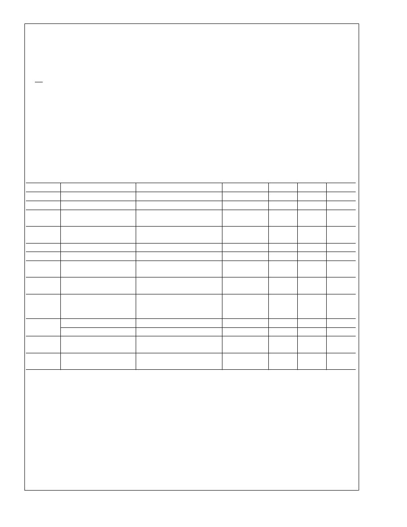
Electrical Characteristics
Limits with standard typeface apply for T
J
= 25C, and limits in
boldface type
apply over the full temperature range. Unless
otherwise specified V
IN
= 3.6V, C
1
= C
2
= C
3
= 1μF.
Symbol
Parameter
Conditions
I
Q
Supply Current
Open Circuit, No Load
I
SD
Shutdown Supply Current
F
SW
Switching Frequency
(Note 5)
η
POWER
Power Efficiency at V
NEG
I
L
= 3.6mA
I
L
= 10mA
T
START
Start Up time
R
NEG
Output Resistance to V
NEG
(Note 6)
V
R
Output Voltage Ripple
(Note 7)
I
L
= 10mA, V
OUT
= 3.8V
V
FB
Feedback Pin Reference
Voltage
V
OUT
Adjustable Output Voltage
5.5V
≥
V
IN
≥
2.7V, 2.5mA
≥
I
L
5.5V
≥
V
IN
≥
3.0V, 10mA
≥
I
L
≥
0mA
Load Regulation
0 to 10mA, V
OUT
= 2.4V
Line Regulation
5.5V
≥
V
IN
≥
2.7V, I
L
= 2.5mA
V
IH
Shutdown Pin Input Voltage
High
V
IL
Shutdown Pin Input Voltage
Low
Min
Typ
400
0.05
260
Max
950
1
450
Units
μA
μA
V
IN
= 3.6V
140
kHz
94
91
120
30
%
600
μs
I
L
=2.5mA, V
OUT
= 2.7V
1
mV
I
L
= 2.5mA (Note 8)
1.25
1.20
1.15
V
(V
IN
0.3V)
(V
IN
1.2V)
V
5
1
mV/mA
mV/V
V
5.5V
≥
V
IN
≥
2.7V
2.4
5.5V
≥
V
IN
≥
2.7V
0.8
V
Note 1:
Absolute Maximum Ratings indicate limits beyond which damage to the device may occur. Electrical specifications do not apply when operating the device
beyond its rated operating conditions.
Note 2:
OUT may be shorted to GND for one second without damage. However, shorting OUT to V
IN
may damage the device and must be avoided. Also, for
temperatures above T
A
= 85C, OUT must not be shorted to GND or V
IN
or device may be damaged.
Note 3:
The maximum power dissipation must be de-rated at elevated temperatures and is limited by T
(maximum junction temperature), T
A
(ambient
temperature) and
θ
JA
(junction-to-ambient thermal resistance). The maximum power dissipation at any temperature is:
PDiss
MAX
= (T
JMAX
— T
A
)/
θ
JA
up to the value listed in the Absolute Maximum Ratings.
Note 4:
Rating is for the human body model, a 100pF capacitor discharged through a 1.5 k
resistor into each pin.
Note 5:
The output switches operate at one half the oscillator frequency, f
OSC
= 2f
SW
.
Note 6:
Current drawn from V
NEG
pin decreases power efficiency and will increase output voltage ripple.
Note 7:
In the test circuit, capacitors C
, C
2
, and C
3
are 1μF, 0.30
maximum ESR capacitors. Capacitors with higher ESR will increase output resistance, increase
output voltage ripple, and reduce efficiency.
Note 8:
The feedback resistors R1 and R2 are 200k
resistors.
L
www.national.com
3
相關(guān)PDF資料 |
PDF描述 |
|---|---|
| LM2787BPX | Low Noise Regulated Switched Capacitor Voltage |
| LM2787BP | Low Noise Regulated Switched Capacitor Voltage |
| LM2788MM-1.5 | 120mA High Efficiency Step-Down Switched Capacitor Voltage Converter |
| LM2788MM-2.0 | 120mA High Efficiency Step-Down Switched Capacitor Voltage Converter |
| LM2788MMX-1.5 | 120mA High Efficiency Step-Down Switched Capacitor Voltage Converter |
相關(guān)代理商/技術(shù)參數(shù) |
參數(shù)描述 |
|---|---|
| LM2787AUP E WAF | 制造商:Texas Instruments 功能描述: |
| LM2787AUPN E WAF | 制造商:Texas Instruments 功能描述: |
| LM2787BP | 制造商:Texas Instruments 功能描述:INVERTER REG SW CAP REG SMD 2787 |
| LM2787BP/NOPB | 功能描述:IC REG SWITCHD CAP INV ADJ 8USMD RoHS:是 類別:集成電路 (IC) >> PMIC - 穩(wěn)壓器 - DC DC 開關(guān)穩(wěn)壓器 系列:- 產(chǎn)品培訓(xùn)模塊:Lead (SnPb) Finish for COTS Obsolescence Mitigation Program 標(biāo)準(zhǔn)包裝:1 系列:- 類型:降壓(降壓) 輸出類型:固定 輸出數(shù):1 輸出電壓:3.3V 輸入電壓:4.5 V ~ 24 V PWM 型:- 頻率 - 開關(guān):- 電流 - 輸出:125mA 同步整流器:無 工作溫度:-40°C ~ 85°C 安裝類型:表面貼裝 封裝/外殼:SOT-23-6 包裝:Digi-Reel® 供應(yīng)商設(shè)備封裝:SOT-6 其它名稱:MAX1836EUT33#TG16DKR |
| LM2787BPEV | 功能描述:電源管理IC開發(fā)工具 EVAL UNIT FOR LM2787 RoHS:否 制造商:Maxim Integrated 產(chǎn)品:Evaluation Kits 類型:Battery Management 工具用于評估:MAX17710GB 輸入電壓: 輸出電壓:1.8 V |
發(fā)布緊急采購,3分鐘左右您將得到回復(fù)。