- 您現(xiàn)在的位置:買賣IC網(wǎng) > PDF目錄358827 > LM2679S-3.3 (NATIONAL SEMICONDUCTOR CORP) SIMPLE SWITCHER 5A Step-Down Voltage Regulator with Adjustable Current Limit PDF資料下載
參數(shù)資料
| 型號: | LM2679S-3.3 |
| 廠商: | NATIONAL SEMICONDUCTOR CORP |
| 元件分類: | 穩(wěn)壓器 |
| 英文描述: | SIMPLE SWITCHER 5A Step-Down Voltage Regulator with Adjustable Current Limit |
| 中文描述: | 8.1 A SWITCHING REGULATOR, 280 kHz SWITCHING FREQ-MAX, PSSO7 |
| 封裝: | TO-263, 7 PIN |
| 文件頁數(shù): | 9/24頁 |
| 文件大小: | 355K |
| 代理商: | LM2679S-3.3 |

Application Hints
The LM2679 provides all of the active functions required for
a step-down (buck) switching regulator. The internal power
switch is a DMOS power MOSFET to provide power supply
designs with high current capability, up to 5A, and highly ef-
ficient operation.
The LM2679 is part of the
SIMPLE SWITCHER
family of
power converters. A complete design uses a minimum num-
ber
of
external
components,
pre-determined from a variety of manufacturers. Using either
this data sheet or a design software program called
LM267X
Made Simple
(version 2.0) a complete switching power sup-
ply can be designed quickly. The software is provided free of
charge and can be downloaded from National Semiconduc-
tor’s Internet site located at http://www.national.com.
PIN 1 - Switch Output
This is the output of a power MOSFET switch connected di-
rectly to the input voltage. The switch provides energy to an
inductor, an output capacitor and the load circuitry under
control of an internal pulse-width-modulator (PWM). The
PWM controller is internally clocked by a fixed 260KHz oscil-
lator. In a standard step-down application the duty cycle
(Time ON/Time OFF) of the power switch is proportional to
the ratio of the power supply output voltage to the input volt-
age. The voltage on pin 1 switches between Vin (switch ON)
and below ground by the voltage drop of the external Schot-
tky diode (switch OFF).
PIN 2 - Input
The input voltage for the power supply is connected to pin 2.
In addition to providing energy to the load the input voltage
also provides bias for the internal circuitry of the LM2679.
For guaranteed performance the input voltage must be in the
range of 8V to 40V. For best performance of the power sup-
ply the input pin should always be bypassed with an input ca-
pacitor located close to pin 2.
PIN 3 - C Boost
A capacitor must be connected from pin 3 to the switch out-
put, pin 1. This capacitor boosts the gate drive to the internal
MOSFET above Vin to fully turn it ON. This minimizes con-
which
have
been
duction losses in the power switch to maintain high effi-
ciency. The recommended value for C Boost is 0.01μF.
PIN 4 - Ground
This is the ground reference connection for all components
in the power supply. In fast-switching, high-current applica-
tions such as those implemented with the LM2679, it is rec-
ommended that a broad ground plane be used to minimize
signal coupling throughout the circuit
PIN 5 - Current Adjust
A key feature of the LM2679 is the ability to tailor the peak
switch current limit to a level required by a particular applica-
tion. This alleviates the need to use external components
that must be physically sized to accommodate current levels
(under shorted output conditions for example) that may be
much higher than the normal circuit operating current re-
quirements.
A resistor connected from pin 5 to ground establishes a cur-
rent (I
= 1.2V / R
) that sets the peak current through
the power switch. The maximum switch current is fixed at a
level of 37,125 / R
ADJ
.
PIN 6 - Feedback
This is the input to a two-stage high gain amplifier, which
drives the PWM controller. It is necessary to connect pin 6 to
the actual output of the power supply to set the dc output
voltage. For the fixed output devices (3.3V, 5V and 12V out-
puts), a direct wire connection to the output is all that is re-
quired as internal gain setting resistors are provided inside
the LM2679. For the adjustable output version two external
resistors are required to set the dc output voltage. For stable
operation of the power supply it is important to prevent cou-
pling of any inductor flux to the feedback input.
PIN 7 - Softstart
A capacitor connected from pin 7 to ground allows for a slow
turn-on of the switching regulator. The capacitor sets a time
delay to gradually increase the duty cycle of the internal
power switch. This can significantly reduce the amount of
surge current required from the input supply during an abrupt
application of the input voltage. If softstart is not required this
pin should be left open circuited.
DESIGN CONSIDERATIONS
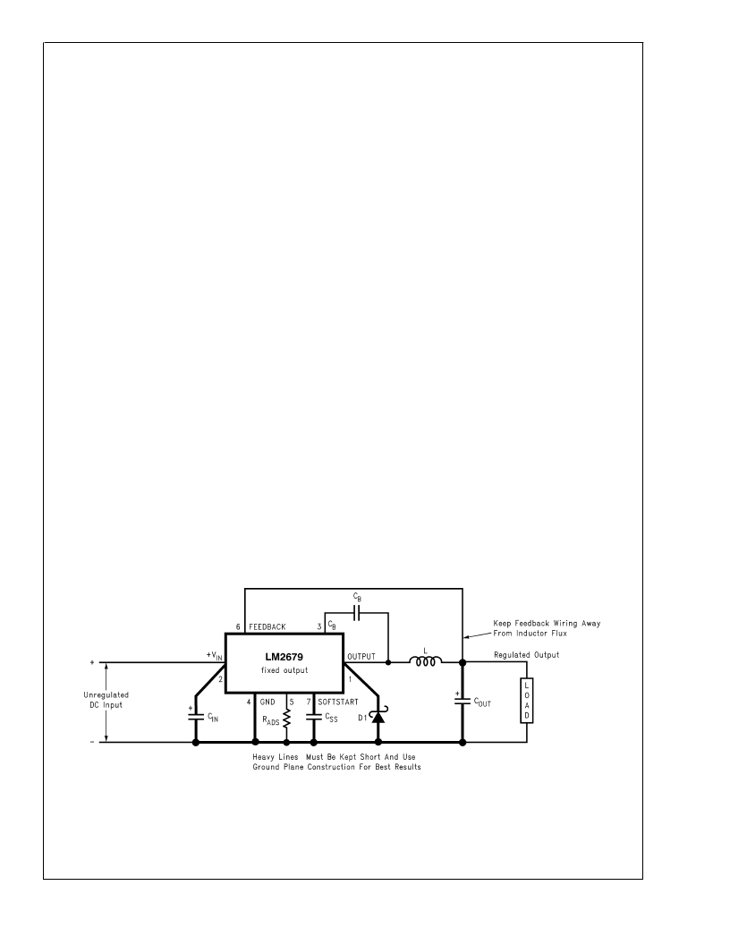
DS100847-23
FIGURE 1. Basic circuit for fixed output voltage applications.
L
www.national.com
9
相關PDF資料 |
PDF描述 |
|---|---|
| LM2679S-5.0 | SIMPLE SWITCHER 5A Step-Down Voltage Regulator with Adjustable Current Limit |
| LM2679T-12 | 392 Series Industrial Potentiometer, Conductive Plastic Element, PC Terminals, 0.5 W Power Rating, 250 Ohm Resistance Value |
| LM2679T-3.3 | 392 Series Industrial Potentiometer, Conductive Plastic Element, PC Terminals, 0.5 W Power Rating, 2.5 kOhm Resistance Value |
| LM2679T-5.0 | SIMPLE SWITCHER 5A Step-Down Voltage Regulator with Adjustable Current Limit |
| LM2679T-ADJ | 392 Series Industrial Potentiometer, Conductive Plastic Element, PC Terminals, 0.5 W Power Rating, 500 Ohm Resistance Value |
相關代理商/技術參數(shù) |
參數(shù)描述 |
|---|---|
| LM2679S-5.0 | 功能描述:直流/直流開關轉換器 RoHS:否 制造商:STMicroelectronics 最大輸入電壓:4.5 V 開關頻率:1.5 MHz 輸出電壓:4.6 V 輸出電流:250 mA 輸出端數(shù)量:2 最大工作溫度:+ 85 C 安裝風格:SMD/SMT |
| LM2679S-5.0/NOPB | 功能描述:直流/直流開關轉換器 5A STEP-DOWN VLTG REG RoHS:否 制造商:STMicroelectronics 最大輸入電壓:4.5 V 開關頻率:1.5 MHz 輸出電壓:4.6 V 輸出電流:250 mA 輸出端數(shù)量:2 最大工作溫度:+ 85 C 安裝風格:SMD/SMT |
| LM2679S5.0NOPB | 制造商:National Semiconductor 功能描述:Conv DC-DC Single Step Down 8V to 40V 8-Pin(7+Tab) TO-263 Rail |
| LM2679S50 | 制造商:Texas Instruments 功能描述:SWITCHING REG 5A 5.0V SMD 2679 |
| LM2679SADJ | 制造商:Texas Instruments 功能描述: |
發(fā)布緊急采購,3分鐘左右您將得到回復。