- 您現(xiàn)在的位置:買賣IC網 > PDF目錄369787 > LM2672LDX-5.0 PDF資料下載
參數(shù)資料
| 型號: | LM2672LDX-5.0 |
| 文件頁數(shù): | 17/25頁 |
| 文件大小: | 495K |
| 代理商: | LM2672LDX-5.0 |

LM2671 Series Buck Regulator Design Procedure (Fixed Output)
(Continued)
LM2671 Series Buck Regulator Design Procedure (Adjustable Output)
PROCEDURE (Adjustable Output Voltage Version)
To simplify the buck regulator design procedure, National
Semiconductor is making available computer design software to
be used with the SIMPLE SWITCHER line of switching
regulators.
LM267X Made Simple
is available on (version 6.0)
Windows 3.1, NT, or 95 operating systems.
Given:
V
OUT
= Regulated Output Voltage
V
IN
(max) = Maximum Input Voltage
I
LOAD
(max) = Maximum Load Current
F = Switching Frequency (Fixed at a nominal 260 kHz).
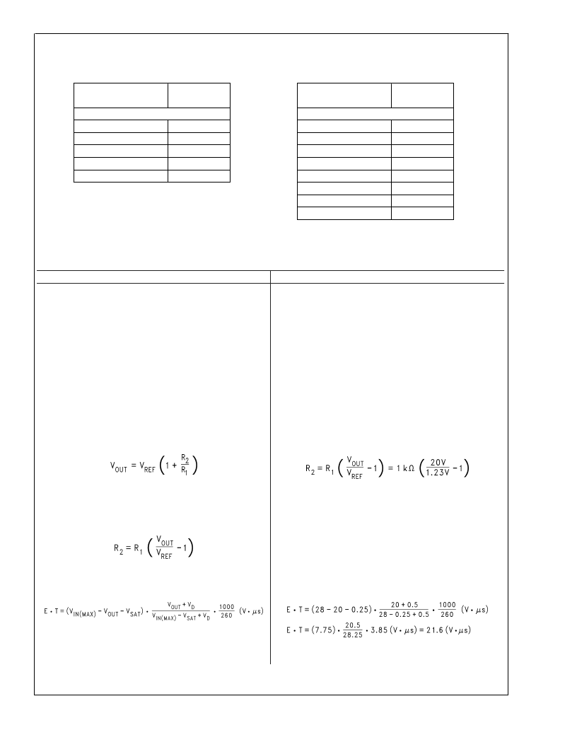
1. Programming Output Voltage
(Selecting R
1
and R
2
, as
shown in Figure 3)
Use the following formula to select the appropriate resistor
values.
EXAMPLE (Adjustable Output Voltage Version)
Given:
V
OUT
= 20V
V
IN
(max) = 28V
I
LOAD
(max) = 500 mA
F = Switching Frequency (Fixed at a nominal 260 kHz).
1. Programming Output Voltage
(Selecting R
1
and R
2
, as
shown in Figure 3)
Select R
1
to be 1 k
, 1%. Solve for R
2
.
where V
REF
= 1.21V
Select a value for R
1
between 240
and 1.5 k
. The lower
resistor values minimize noise pickup in the sensitive feedback
pin. (For the lowest temperature coefficient and the best stability
with time, use 1% metal film resistors.)
R
2
= 1 k
(16.53 1) = 15.53 k
, closest 1% value is 15.4 k
.
R
2
= 15.4 k
.
2. Inductor Selection (L1)
A.
Calculate the inductor Volt
microsecond constant E
T
(V
μs), from the following formula:
2. Inductor Selection (L1)
A.
Calculate the inductor Volt
microsecond constant (E
T),
where V
SAT
=internal switch saturation voltage=0.25V and
V
D
= diode forward voltage drop = 0.5V
AVX TPS
Recommended
Application Voltage
Voltage
Rating
+85C Rating
3.3
5
10
12
15
6.3
10
20
25
35
Sprague 594D
Recommended
Application Voltage
Voltage
Rating
+85C Rating
2.5
3.3
5
8
12
18
24
29
4
6.3
10
16
20
25
35
50
FIGURE 15. Recommended Application Voltage for AVX TPS and
Sprague 594D Tantalum Chip Capacitors Derated for 85C.
L
www.national.com
17
相關PDF資料 |
PDF描述 |
|---|---|
| LM2672LDX-ADJ | |
| LM2672MX-12 | |
| LM2672MX-3.3 | |
| LM2672MX-5.0 | |
| LM2672MX-ADJ | |
相關代理商/技術參數(shù) |
參數(shù)描述 |
|---|---|
| LM2672LDX-ADJ | 制造商:未知廠家 制造商全稱:未知廠家 功能描述: |
| LM2672M-12 | 功能描述:直流/直流開關轉換器 RoHS:否 制造商:STMicroelectronics 最大輸入電壓:4.5 V 開關頻率:1.5 MHz 輸出電壓:4.6 V 輸出電流:250 mA 輸出端數(shù)量:2 最大工作溫度:+ 85 C 安裝風格:SMD/SMT |
| LM2672M-12/NOPB | 功能描述:直流/直流開關轉換器 HIGH EFF 1A STEP- DOWN VLTG REG RoHS:否 制造商:STMicroelectronics 最大輸入電壓:4.5 V 開關頻率:1.5 MHz 輸出電壓:4.6 V 輸出電流:250 mA 輸出端數(shù)量:2 最大工作溫度:+ 85 C 安裝風格:SMD/SMT |
| LM2672M-12NOPB | 制造商:Texas Instruments 功能描述: |
| LM2672M-3.3 | 功能描述:直流/直流開關轉換器 RoHS:否 制造商:STMicroelectronics 最大輸入電壓:4.5 V 開關頻率:1.5 MHz 輸出電壓:4.6 V 輸出電流:250 mA 輸出端數(shù)量:2 最大工作溫度:+ 85 C 安裝風格:SMD/SMT |
發(fā)布緊急采購,3分鐘左右您將得到回復。