- 您現(xiàn)在的位置:買賣IC網(wǎng) > PDF目錄361024 > LM2598T-3.3 (NATIONAL SEMICONDUCTOR CORP) SIMPLE SWITCHER Power Converter 150 kHz 1A Step-Down Voltage Regulator, with Features PDF資料下載
參數(shù)資料
| 型號: | LM2598T-3.3 |
| 廠商: | NATIONAL SEMICONDUCTOR CORP |
| 元件分類: | 穩(wěn)壓器 |
| 英文描述: | SIMPLE SWITCHER Power Converter 150 kHz 1A Step-Down Voltage Regulator, with Features |
| 中文描述: | 2.6 A SWITCHING REGULATOR, 173 kHz SWITCHING FREQ-MAX, PSFM7 |
| 封裝: | BENT STAGGERED, TO-220, 7 PIN |
| 文件頁數(shù): | 5/33頁 |
| 文件大?。?/td> | 847K |
| 代理商: | LM2598T-3.3 |
第1頁第2頁第3頁第4頁當前第5頁第6頁第7頁第8頁第9頁第10頁第11頁第12頁第13頁第14頁第15頁第16頁第17頁第18頁第19頁第20頁第21頁第22頁第23頁第24頁第25頁第26頁第27頁第28頁第29頁第30頁第31頁第32頁第33頁
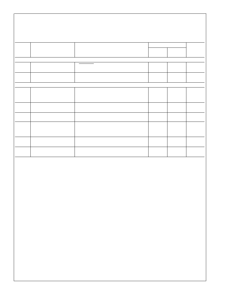
All Output Voltage Versions
Electrical Characteristics
(Continued)
Specifications with standard type face are for T
J
= 25C, and those with
boldface type
apply over
full Operating Tempera-
ture Range
. Unless otherwise specified, V
IN
= 12V for the 3.3V, 5V, and Adjustable version and V
IN
= 24V for the 12V ver-
sion. I
LOAD
= 200 mA
Symbol
Parameter
Conditions
LM2598-XX
Typ
(Note 4)
Units
(Limits)
Limit
(Note 5)
SHUTDOWN/SOFT-START CONTROL
Test Circuit of Figure 1
I
SD
Shutdown Current
V
SHUTDOWN
= 0.5V
5
μA
10
μA(max)
μA
μA(max)
I
SS
Soft-start Current
V
Soft-start
= 2.5V
1.6
5
FLAG/DELAY CONTROL
Test Circuit of Figure 1
Regulator Dropout Detector
Threshold Voltage
Low (Flag ON)
96
%
92
98
%(min)
%(max)
V
V(max)
μA
VF
SAT
Flag Output Saturation
Voltage
Flag Output Leakage
Current
Delay Pin Threshold
Voltage
I
SINK
= 3 mA
V
DELAY
= 0.5V
V
FLAG
= 40V
0.3
0.7/
1.0
IF
L
0.3
1.25
V
Low (Flag ON)
High (Flag OFF) and V
OUT
Regulated
V
DELAY
= 0.5V
1.21
1.29
V(min)
V(max)
μA
μA(max)
mV
mV(max)
Delay Pin Source Current
3
6
Delay Pin Saturation
Low (Flag ON)
55
350/
400
Note 1:
Absolute Maximum Ratings indicate limits beyond which damage to the device may occur. Operating Ratings indicate conditions for which the device is
intended to be functional, but do not guarantee specific performance limits. For guaranteed specifications and test conditions, see the Electrical Characteristics.
Note 2:
Voltage internally clamped. If clamp voltage is exceeded, limit current to a maximum of 1 mA.
Note 3:
The human body model is a 100 pF capacitor discharged through a 1.5k resistor into each pin.
Note 4:
Typical numbers are at 25C and represent the most likely norm.
Note 5:
All limits guaranteed at room temperature (standard type face) and at
temperature extremes (bold type face).
All room temperature limits are 100%
production tested. All limits at
temperature extremes
are guaranteed via correlation using standard Statistical Quality Control (SQC) methods. All limits are used
to calculate Average Outgoing Quality Level (AOQL).
Note 6:
External components such as the catch diode, inductor, input and output capacitors can affect switching regulator system performance. When the LM2598
is used as shown in the Figure 1 test circuit, system performance will be as shown in system parameters section of Electrical Characteristics.
Note 7:
The switching frequency is reduced when the second stage current limit is activated. The amount of reduction is determined by the severity of current
overload.
Note 8:
No diode, inductor or capacitor connected to output pin.
Note 9:
Feedback pin removed from output and connected to 0V to force the output transistor switch ON.
Note 10:
Feedback pin removed from output and connected to 12V for the 3.3V, 5V, and theADJ. version, and 15V for the 12V version, to force the output transistor
switch OFF.
Note 11:
V
IN
= 40V.
Note 12:
Junction to ambient thermal resistance (no external heat sink) for the TO-220 package mounted vertically, with the leads soldered to a printed circuit board
with (1 oz.) copper area of approximately 1 in
.
Note 13:
Junction to ambient thermal resistance with the TO-263 package tab soldered to a single sided printed circuit board with 0.5 in
2
of (1 oz.) copper area.
Note 14:
Junction to ambient thermal resistance with the TO-263 package tab soldered to a single sided printed circuit board with 2.5 in
2
of (1 oz.) copper area.
Note 15:
Junction to ambient thermal resistance with the TO-263 package tab soldered to a double sided printed circuit board with 3 in
2
of (1 oz.) copper area on
the LM2598S side of the board, and approximately 16 in
of copper on the other side of the p-c board. See application hints in this data sheet and the thermal model
in
Switchers Made Simple
version 4.2 software.
L
www.national.com
5
相關(guān)PDF資料 |
PDF描述 |
|---|---|
| LM2598T-5.0 | SIMPLE SWITCHER Power Converter 150 kHz 1A Step-Down Voltage Regulator, with Features |
| LM2598T-ADJ | SIMPLE SWITCHER Power Converter 150 kHz 1A Step-Down Voltage Regulator, with Features |
| LM2598 | SIMPLE SWITCHER Power Converter 150 kHz 1A Step-Down Voltage Regulator, with Features |
| LM2598S-5.0 | SIMPLE SWITCHER Power Converter 150 kHz 1A Step-Down Voltage Regulator, with Features |
| LM2598S-12 | SIMPLE SWITCHER Power Converter 150 kHz 1A Step-Down Voltage Regulator, with Features |
相關(guān)代理商/技術(shù)參數(shù) |
參數(shù)描述 |
|---|---|
| LM2598T-5.0 | 功能描述:直流/直流開關(guān)轉(zhuǎn)換器 RoHS:否 制造商:STMicroelectronics 最大輸入電壓:4.5 V 開關(guān)頻率:1.5 MHz 輸出電壓:4.6 V 輸出電流:250 mA 輸出端數(shù)量:2 最大工作溫度:+ 85 C 安裝風(fēng)格:SMD/SMT |
| LM2598T-5.0/NOPB | 功能描述:直流/直流開關(guān)轉(zhuǎn)換器 RoHS:否 制造商:STMicroelectronics 最大輸入電壓:4.5 V 開關(guān)頻率:1.5 MHz 輸出電壓:4.6 V 輸出電流:250 mA 輸出端數(shù)量:2 最大工作溫度:+ 85 C 安裝風(fēng)格:SMD/SMT |
| LM2598T-ADJ | 功能描述:直流/直流開關(guān)轉(zhuǎn)換器 RoHS:否 制造商:STMicroelectronics 最大輸入電壓:4.5 V 開關(guān)頻率:1.5 MHz 輸出電壓:4.6 V 輸出電流:250 mA 輸出端數(shù)量:2 最大工作溫度:+ 85 C 安裝風(fēng)格:SMD/SMT |
| LM2598T-ADJ/NOPB | 功能描述:直流/直流開關(guān)轉(zhuǎn)換器 RoHS:否 制造商:STMicroelectronics 最大輸入電壓:4.5 V 開關(guān)頻率:1.5 MHz 輸出電壓:4.6 V 輸出電流:250 mA 輸出端數(shù)量:2 最大工作溫度:+ 85 C 安裝風(fēng)格:SMD/SMT |
| LM2599S-12 | 功能描述:直流/直流開關(guān)轉(zhuǎn)換器 RoHS:否 制造商:STMicroelectronics 最大輸入電壓:4.5 V 開關(guān)頻率:1.5 MHz 輸出電壓:4.6 V 輸出電流:250 mA 輸出端數(shù)量:2 最大工作溫度:+ 85 C 安裝風(fēng)格:SMD/SMT |
發(fā)布緊急采購,3分鐘左右您將得到回復(fù)。