- 您現(xiàn)在的位置:買賣IC網(wǎng) > PDF目錄384596 > LM20134MHE (NATIONAL SEMICONDUCTOR CORP) 4A, PowerWise㈢ Synchronous Buck Regulator with Input Synchronization PDF資料下載
參數(shù)資料
| 型號: | LM20134MHE |
| 廠商: | NATIONAL SEMICONDUCTOR CORP |
| 元件分類: | 穩(wěn)壓器 |
| 英文描述: | 4A, PowerWise㈢ Synchronous Buck Regulator with Input Synchronization |
| 中文描述: | 7.9 A SWITCHING REGULATOR, 460 kHz SWITCHING FREQ-MAX, PDSO16 |
| 封裝: | TSSOP-16 |
| 文件頁數(shù): | 15/22頁 |
| 文件大?。?/td> | 608K |
| 代理商: | LM20134MHE |
To achieve a -20dB/decade slope, the error amplifier zero,
located at f
, should positioned to cancel the output filter
pole (f
). An additional error amp pole, located at f
,
can be added to cancel the output filter zero at (f
). Can-
cellation of the output filter zero is recommended if larger
value, non-ceramic output capacitors are used.
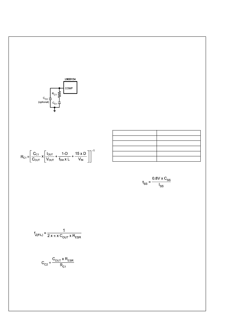
Compensation of the LM20134 is achieved by adding an RC
network as shown in
Figure 5
below.
30030414
FIGURE 5. Compensation Network for LM20134
A good starting value for C
for most applications is 4.7 nF.
Once the value of C
is chosen the value of RC should be
calculated using the equation below to cancel the output filter
pole (f
P(FIL)
) as shown in
Figure 4
.
A higher crossover frequency can be obtained, usually at the
expense of phase margin, by lowering the value of C
C1
and
recalculating the value of R
. Likewise, increaseing C
and
recalculating R
will provide additional phase margin at a
lower crossover frequency. As with any attempt to compen-
sate the LM20134 the stability of the system should be verified
for desired transient droop and settling time.
If the output filter zero, (f
) approaches the crossover fre-
quency (F
), an additional capacitor (C
) should be placed
at the COMP pin to ground. This capacitor adds a pole to
cancel the output filter zero assuring the crossover frequency
will occur before the double pole at f
/2 degrades the phase
margin. The output filter zero is set by the output capacitor
value and ESR as shown in the equation below.
If needed, the value for C
C2
should be calculated using the
equation shown below.
Where R
is the output capacitor series resistance and
R
C1
is the calculated compensation resistance.
AVIN FILTERING COMPONENTS (C
F
and R
F
)
To prevent high frequency noise spikes from disturbing the
sensitive analog circuitry connected to the AVIN and AGND
pins, a high frequency RC filter is required between PVIN and
AVIN. These components are shown in
Figure 2
as C
F
and
R
. The required value for R
is 1
. C
must be used. Rec-
ommended value of C
is 1.0 μF. The filter capacitor, C
F
should be placed as close to the IC as possible with a direct
connection from AVIN to AGND. A good quality X5R or X7R
ceramic capacitor should be used for C
F
.
SUB-REGULATOR BYPASS CAPACITOR (C
VCC
)
The capacitor at the VCC pin provides noise filtering and sta-
bility for the internal sub-regulator. The recommended value
of C
should be no smaller than 1 μF and no greater than
10 μF. The capacitor should be a good quality ceramic X5R
or X7R capacitor. In general, a 1 μF ceramic capacitor is rec-
ommended for most applications.
SETTING THE START UP TIME (C
SS
)
The addition of a capacitor connected from the SS pin to
ground sets the time at which the output voltage will reach the
final regulated value. Larger values for C
will result in longer
start up times. Table 3, shown below provides a list of soft
start capacitors and the corresponding typical start up times.
TABLE 3. Start Up Times for Different Soft-Start
Capacitors
Start Up Time (ms)
C
SS
(nF)
none
33
68
100
120
1
5
10
15
20
If different start up times are needed the equation shown be-
low can be used to calculate the start up time.
As shown above, the start up time is influenced by the value
of the Soft-Start capacitor C
(F) and the 5 μA Soft-Start pin
current I
SS
(A). that may be found in the electrical character-
istics table.
While the Soft-Start capacitor can be sized to meet many start
up requirements, there are limitations to its size. The Soft-
Start time can never be faster than 1ms due to the internal
default 1ms start up time. When the device is enabled there
is an approximate time interval of 50 μs when the Soft-Start
capacitor will be discharged just prior to the Soft-Start ramp.
If the enable pin is rapidly pulsed or the Soft-Start capacitor
is large there may not be enough time for C
to completely
discharge resulting in start up times less than predicted. To
aid in discharging the Soft-Start capacitor during long disable
periods an external 1 M
resistor from SS/TRK to ground can
be used without greatly affecting the start-up time.
USING PRECISION ENABLE AND POWER GOOD
The precision enable(EN) and power good(PGOOD) pins of
the LM20134 can be used to address many sequencing re-
quirements. The turn-on of the LM20134 can be controlled
with the precision enable pin by using two external resistors
as shown in
Figure 6
15
www.national.com
L
相關(guān)PDF資料 |
PDF描述 |
|---|---|
| LM20134MHX | 4A, PowerWise㈢ Synchronous Buck Regulator with Input Synchronization |
| LM20144 | 4A, PowerWise㈢ Adjustable Frequency Synchronous Buck Regulator |
| LM20144MH | 4A, PowerWise㈢ Adjustable Frequency Synchronous Buck Regulator |
| LM20144MHE | 4A, PowerWise㈢ Adjustable Frequency Synchronous Buck Regulator |
| LM20144MHX | 4A, PowerWise㈢ Adjustable Frequency Synchronous Buck Regulator |
相關(guān)代理商/技術(shù)參數(shù) |
參數(shù)描述 |
|---|---|
| LM20134MHE/NOPB | 功能描述:直流/直流開關(guān)轉(zhuǎn)換器 RoHS:否 制造商:STMicroelectronics 最大輸入電壓:4.5 V 開關(guān)頻率:1.5 MHz 輸出電壓:4.6 V 輸出電流:250 mA 輸出端數(shù)量:2 最大工作溫度:+ 85 C 安裝風(fēng)格:SMD/SMT |
| LM20134MHX | 制造商:NSC 制造商全稱:National Semiconductor 功能描述:4A, PowerWise㈢ Synchronous Buck Regulator with Input Synchronization |
| LM20134MHX/NOPB | 功能描述:直流/直流開關(guān)轉(zhuǎn)換器 RoHS:否 制造商:STMicroelectronics 最大輸入電壓:4.5 V 開關(guān)頻率:1.5 MHz 輸出電壓:4.6 V 輸出電流:250 mA 輸出端數(shù)量:2 最大工作溫度:+ 85 C 安裝風(fēng)格:SMD/SMT |
| LM20134Q | 制造商:TI 制造商全稱:Texas Instruments 功能描述:LM20134/LM20134Q 4A, PowerWise Synchronous Buck Regulator with Input |
| LM20136 | 制造商:NSC 制造商全稱:National Semiconductor 功能描述:6A, Synchronous Buck Regulator with Input Synchronization |
發(fā)布緊急采購,3分鐘左右您將得到回復(fù)。