- 您現(xiàn)在的位置:買(mǎi)賣(mài)IC網(wǎng) > PDF目錄361023 > LM1770SMFX (NATIONAL SEMICONDUCTOR CORP) SOT-23 Synchronous Buck Controller PDF資料下載
參數(shù)資料
| 型號(hào): | LM1770SMFX |
| 廠商: | NATIONAL SEMICONDUCTOR CORP |
| 元件分類(lèi): | 穩(wěn)壓器 |
| 英文描述: | SOT-23 Synchronous Buck Controller |
| 中文描述: | SWITCHING CONTROLLER, 1000 kHz SWITCHING FREQ-MAX, PDSO5 |
| 封裝: | SOT-23, 5 PIN |
| 文件頁(yè)數(shù): | 13/14頁(yè) |
| 文件大小: | 687K |
| 代理商: | LM1770SMFX |
第1頁(yè)第2頁(yè)第3頁(yè)第4頁(yè)第5頁(yè)第6頁(yè)第7頁(yè)第8頁(yè)第9頁(yè)第10頁(yè)第11頁(yè)第12頁(yè)當(dāng)前第13頁(yè)第14頁(yè)
Efficiency Calculations
(Continued)
SWITCHING LOSS
The next loss is the switching loss that is caused by the need
to charge and discharge the gate capacitance of the FETs
every cycle. This can be approximated by:
P
P_SWITCH
= V
IN
x Q
g_PMOS
x f
SW
for the PMOS, and the same approach can be adapted for
the NMOS:
P
N_SWITCH
= V
IN
x Q
g_NMOS
x f
SW
TRANSITIONAL LOSS
The last FET power loss is the transitional loss. This is
caused by switching the PMOS while it is conducting current.
This approach only models the PMOS transition, the NMOS
loss is considered negligible because it has minimal drain to
source voltage when it switches due to the conduction of the
body diode. Therefore the transitional loss of the PMOS can
be modeled by:
P
P_TRANSITIONAL
= 0.5 x V
IN
x I
OUT
x f
SW
x (t
r
+ t
f
)
t
and t
are the rise and fall times of the FET and can be
found in their corresponding datasheet. Typically these num-
bers are simulated using a 6
drive, which corresponds well
to the LM1770. Given this, no adjustment is needed.
DCR LOSS
The last source of power loss in the system that needs to be
calculated is the loss associated with the inductor resistance
(DCR) which can be calculated by
P
DCR
= R
DCR
x I
OUT2
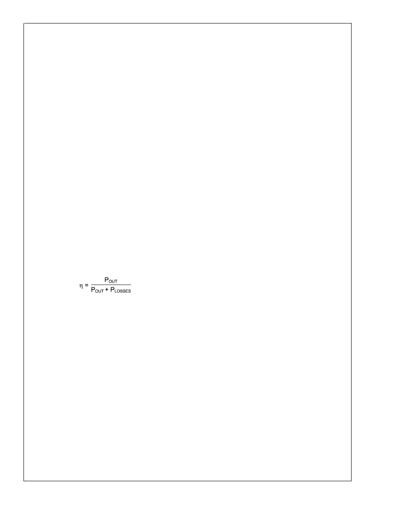
EFFICIENCY
The efficiency,
η
, can then be calculated by summing all the
power losses and then using the equation below:
Thermals
By breaking down the individual power loss in each compo-
nent it makes it easy to determine the temperature rise of
each component. Generally the expected temperature rise
of the LM1770 is extremely low as it is not in the power path.
Therefore the only two items of concern are the PMOS and
the NMOS. The power loss in the PMOS is the sum of the
conduction loss and transitional loss, while the NMOS only
has conduction loss. It is assumed that any loss associated
with the body diode conduction during the dead-time is
negligible.
For completeness of design it is important to watch out for
the temperature rise of the inductor.Assuming the inductor is
kept out of saturation the predominant loss will be the DC
copper resistance. At higher frequencies, depending on the
core material, the core loss could approach or exceed the
DCR losses. Consult with the inductor manufacturer for ap-
propriate temp curves based on current.
Layout
The LM1770, like all switching regulators, requires careful
attention to layout to ensure optimal performance. The fol-
lowing steps should be taken to aid in the layout. For more
information refer to Application Note AN-1299.
1.
Ensure that the ground connections of the input capaci-
tor, output capacitor and NMOS are as close as pos-
sible. Ideally these should all be grounded together in
close proximity on the component side of the board.
2.
Keep the switch node small to minimize EMI without
degrading thermal cooling of the FETs.
3.
Locate the feedback resistors close to the IC and keep
the feedback trace as short as possible. Do not run any
feedback traces near the switch node.
4.
Keep the gate traces short and keep them away from the
switch node as much as possible.
5.
If a small bypass capacitor is used on V
IN
(0.1μF) place
it as close to the pin, with the ground connection as
close to the chip ground as possible.
L
www.national.com
13
相關(guān)PDF資料 |
PDF描述 |
|---|---|
| LM1770TMF | SOT-23 Synchronous Buck Controller |
| LM1770 | SOT-23 Synchronous Buck Controller |
| LM1770TMFX | SOT-23 Synchronous Buck Controller |
| LM2002 | CONN HEADER 18POS .100 VERT GOLD |
| LM2002AT | 8 Watt Audio Power Amplifier |
相關(guān)代理商/技術(shù)參數(shù) |
參數(shù)描述 |
|---|---|
| LM1770SMFX/NOPB | 功能描述:DC/DC 開(kāi)關(guān)控制器 RoHS:否 制造商:Texas Instruments 輸入電壓:6 V to 100 V 開(kāi)關(guān)頻率: 輸出電壓:1.215 V to 80 V 輸出電流:3.5 A 輸出端數(shù)量:1 最大工作溫度:+ 125 C 安裝風(fēng)格: 封裝 / 箱體:CPAK |
| LM1770TMF | 功能描述:DC/DC 開(kāi)關(guān)控制器 RoHS:否 制造商:Texas Instruments 輸入電壓:6 V to 100 V 開(kāi)關(guān)頻率: 輸出電壓:1.215 V to 80 V 輸出電流:3.5 A 輸出端數(shù)量:1 最大工作溫度:+ 125 C 安裝風(fēng)格: 封裝 / 箱體:CPAK |
| LM1770TMF/NOPB | 功能描述:DC/DC 開(kāi)關(guān)控制器 RoHS:否 制造商:Texas Instruments 輸入電壓:6 V to 100 V 開(kāi)關(guān)頻率: 輸出電壓:1.215 V to 80 V 輸出電流:3.5 A 輸出端數(shù)量:1 最大工作溫度:+ 125 C 安裝風(fēng)格: 封裝 / 箱體:CPAK |
| LM1770TMFX | 功能描述:DC/DC 開(kāi)關(guān)控制器 RoHS:否 制造商:Texas Instruments 輸入電壓:6 V to 100 V 開(kāi)關(guān)頻率: 輸出電壓:1.215 V to 80 V 輸出電流:3.5 A 輸出端數(shù)量:1 最大工作溫度:+ 125 C 安裝風(fēng)格: 封裝 / 箱體:CPAK |
| LM1770TMFX/NOPB | 功能描述:DC/DC 開(kāi)關(guān)控制器 RoHS:否 制造商:Texas Instruments 輸入電壓:6 V to 100 V 開(kāi)關(guān)頻率: 輸出電壓:1.215 V to 80 V 輸出電流:3.5 A 輸出端數(shù)量:1 最大工作溫度:+ 125 C 安裝風(fēng)格: 封裝 / 箱體:CPAK |
發(fā)布緊急采購(gòu),3分鐘左右您將得到回復(fù)。