- 您現(xiàn)在的位置:買賣IC網(wǎng) > PDF目錄361023 > LM10CWM (NATIONAL SEMICONDUCTOR CORP) Operational Amplifier and Voltage Reference PDF資料下載
參數(shù)資料
| 型號(hào): | LM10CWM |
| 廠商: | NATIONAL SEMICONDUCTOR CORP |
| 元件分類: | 運(yùn)動(dòng)控制電子 |
| 英文描述: | Operational Amplifier and Voltage Reference |
| 中文描述: | OP-AMP, 5000 uV OFFSET-MAX, PDSO14 |
| 封裝: | PLASTIC, SOP-14 |
| 文件頁(yè)數(shù): | 4/21頁(yè) |
| 文件大小: | 688K |
| 代理商: | LM10CWM |
第1頁(yè)第2頁(yè)第3頁(yè)當(dāng)前第4頁(yè)第5頁(yè)第6頁(yè)第7頁(yè)第8頁(yè)第9頁(yè)第10頁(yè)第11頁(yè)第12頁(yè)第13頁(yè)第14頁(yè)第15頁(yè)第16頁(yè)第17頁(yè)第18頁(yè)第19頁(yè)第20頁(yè)第21頁(yè)
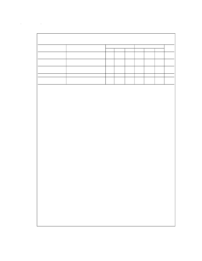
Electrical Characteristics
(Continued)
T
J
=25C,
T
MIN
≤
T
J
≤
T
MAX
(Boldface type refers to limits over temperature range)
(Note 5)
Parameter
Conditions
LM10BL
Typ
70
LM10CL
Typ
70
Units
Min
30
20
195
194
Max
Min
20
15
190
189
Max
Amplifier gain
0.2V
≤
V
REF
≤
5.5V
V/mV
V/mV
mV
mV
nA
nA
%/C
μA
μA
Feedback sense voltage
200
205
206
50
65
200
210
211
75
90
Feedback current
20
22
Reference drift
Supply current
0.002
260
0.003
280
400
500
500
570
Note 1:
Absolute Maximum Ratings indicate limits beyond which damage to the device may occur. Operating Ratings indicate conditions for which the device is func-
tional, but do not guarantee specific performance limits.
Note 2:
The Input voltage can exceed the supply voltages provided that the voltage from the input to any other terminal does not exceed the maximum differential
input voltage and excess dissipation is accounted for when V
IN
V
.
Note 3:
The maximum, operating-junction temperature is 150C for the LM10, 100C for the LM10B(L) and 85C for the LM10C(L).At elevated temperatures, devices
must be derated based on package thermal resistance.
Note 4:
Internal thermal limiting prevents excessive heating that could result in sudden failure, but the IC can be subjected to accelerated stress with a shorted output
and worst-case conditions.
Note 5:
These specifications apply for V
≤
V
≤
V
+
0.85V
(1.0V),
1.2V
(1.3V)
<
V
≤
V
, V
=0.2V and 0
≤
I
≤
1.0 mA, unless otherwise specified: V
=40V
for the standard part and 6.5V for the low voltage part. Normal typeface indicates 25C limits.
Boldface type indicates limits and altered test conditions for
full-temperature-range operation;
this is 55C to 125C for the LM10, 25C to 85C for the LM10B(L) and 0C to 70C for the LM10C(L). The specifications do
not include the effects of thermal gradients (
τ
1
20 ms), die heating (
τ
2
0.2s) or package heating. Gradient effects are small and tend to offset the electrical error (see
curves).
Note 6:
For T
J
>
90C, I
OS
may exceed 1.5 nA for V
CM
=V
. With T
J
=125C and V
≤
V
CM
≤
V
+0.1V, I
OS
≤
5 nA.
Note 7:
This defines operation in floating applications such as the bootstrapped regulator or two-wire transmitter. Output is connected to the V
+
terminal of the IC
and input common mode is referred to V
(see typical applications). Effect of larger output-voltage swings with higher load resistance can be accounted for by adding
the positive-supply rejection error.
Note 8:
Refer to RETS10X for LM10H military specifications.
Definition of Terms
Input offset voltage:
That voltage which must be applied
between the input terminals to bias the unloaded output in
the linear region.
Input offset current:
The difference in the currents at the in-
put terminals when the unloaded output is in the linear re-
gion.
Input bias current:
The absolute value of the average of the
two input currents.
Input resistance:
The ratio of the change in input voltage to
the change in input current on either input with the other
grounded.
Large signal voltage gain:
The ratio of the specified output
voltage swing to the change in differential input voltage re-
quired to produce it.
Shunt gain:
The ratio of the specified output voltage swing
to the change in differential input voltage required to produce
it with the output tied to the V
+
terminal of the IC. The load
and power source are connected between the V
and V
ter-
minals, and input common-mode is referred to the V
termi-
nal.
Common-mode rejection:
The ratio of the input voltage
range to the change in offset voltage between the extremes.
Supply-voltage rejection:
The ratio of the specified
supply-voltage change to the change in offset voltage be-
tween the extremes.
Line regulation:
The average change in reference output
voltage over the specified supply voltage range.
Load regulation:
The change in reference output voltage
from no load to that load specified.
Feedback sense voltage:
The voltage, referred to V
, on
the reference feedback terminal while operating in regula-
tion.
Reference amplifier gain:
The ratio of the specified refer-
ence output change to the change in feedback sense voltage
required to produce it.
Feedback current:
The absolute value of the current at the
feedback terminal when operating in regulation.
Supply current:
The current required from the power
source to operate the amplifier and reference with their out-
puts unloaded and operating in the linear range.
www.national.com
4
相關(guān)PDF資料 |
PDF描述 |
|---|---|
| LM10 | Low Power Op Amp and Reference |
| LM1558H | Dual Operational Amplifier |
| LM1558J | Dual Operational Amplifier |
| LM1558 | Dual Operational Amplifier |
| LM1596H | Balanced Modulator-Demodulator |
相關(guān)代理商/技術(shù)參數(shù) |
參數(shù)描述 |
|---|---|
| LM10CWM/NOPB | 功能描述:運(yùn)算放大器 - 運(yùn)放 OP AMP AND VLTG REF RoHS:否 制造商:STMicroelectronics 通道數(shù)量:4 共模抑制比(最小值):63 dB 輸入補(bǔ)償電壓:1 mV 輸入偏流(最大值):10 pA 工作電源電壓:2.7 V to 5.5 V 安裝風(fēng)格:SMD/SMT 封裝 / 箱體:QFN-16 轉(zhuǎn)換速度:0.89 V/us 關(guān)閉:No 輸出電流:55 mA 最大工作溫度:+ 125 C 封裝:Reel |
| LM10CWM/NOPB | 制造商:Texas Instruments 功能描述:Operational Amplifier (Op-Amp) IC |
| LM10CWMX | 功能描述:運(yùn)算放大器 - 運(yùn)放 RoHS:否 制造商:STMicroelectronics 通道數(shù)量:4 共模抑制比(最小值):63 dB 輸入補(bǔ)償電壓:1 mV 輸入偏流(最大值):10 pA 工作電源電壓:2.7 V to 5.5 V 安裝風(fēng)格:SMD/SMT 封裝 / 箱體:QFN-16 轉(zhuǎn)換速度:0.89 V/us 關(guān)閉:No 輸出電流:55 mA 最大工作溫度:+ 125 C 封裝:Reel |
| LM10CWMX/NOPB | 功能描述:運(yùn)算放大器 - 運(yùn)放 RoHS:否 制造商:STMicroelectronics 通道數(shù)量:4 共模抑制比(最小值):63 dB 輸入補(bǔ)償電壓:1 mV 輸入偏流(最大值):10 pA 工作電源電壓:2.7 V to 5.5 V 安裝風(fēng)格:SMD/SMT 封裝 / 箱體:QFN-16 轉(zhuǎn)換速度:0.89 V/us 關(guān)閉:No 輸出電流:55 mA 最大工作溫度:+ 125 C 封裝:Reel |
| LM10D8 | 制造商:Pulse 功能描述:TRANSFORMERS - Rail/Tube |
發(fā)布緊急采購(gòu),3分鐘左右您將得到回復(fù)。