- 您現(xiàn)在的位置:買賣IC網(wǎng) > PDF目錄377641 > LH1526AB (VISHAY SEMICONDUCTORS) Relay SSR 50mA 1.4V DC-IN 0.25A 400V AC/DC-OUT 8-Pin PDIP Tube PDF資料下載
參數(shù)資料
| 型號: | LH1526AB |
| 廠商: | VISHAY SEMICONDUCTORS |
| 元件分類: | 特殊繼電器 |
| 英文描述: | Relay SSR 50mA 1.4V DC-IN 0.25A 400V AC/DC-OUT 8-Pin PDIP Tube |
| 中文描述: | Solid State Relays Dual Normally Open Form 1A 400V |
| 文件頁數(shù): | 2/7頁 |
| 文件大?。?/td> | 155K |
| 代理商: | LH1526AB |
LH1526AB, LH1526AAC, LH1526AACTR
www.vishay.com
Vishay Semiconductors
Rev. 1.9, 25-Jul-11
2
Document Number: 83825
For technical questions, contact:
optocoupleranswers@vishay.com
THIS DOCUMENT IS SUBJECT TO CHANGE WITHOUT NOTICE. THE PRODUCTS DESCRIBED HEREIN AND THIS DOCUMENT
ARE SUBJECT TO SPECIFIC DISCLAIMERS, SET FORTH AT
www.vishay.com/doc91000
Notes
Stresses in excess of the absolute maximum ratings can cause permanent damage to the device. Functional operation of the device is not
implied at these or any other conditions in excess of those given in the operational sections of this document. Exposure to absolute
maximum ratings for extended periods of the time can adversely affect reliability.
(1)
Refer to reflow profile for soldering conditions for surface mounted devices (SMD). Refer to wave profile for soldering conditions for through
hole devices (DIP).
Note
Minimum and maximum values are testing requirements. Typical values are characteristics of the device and are the result of engineering
evaluations. Typical values are for information only and are not part of the testing requirements.
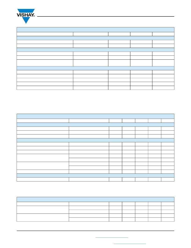
ABSOLUTE MAXIMUM RATINGS
(T
amb
= 25 °C, unless otherwise specified)
PARAMETER
INPUT
LED input ratings: continuous forward current
LED input ratings: reverse voltage
OUTPUT
Output operation: DC or peak AC load voltage
Continuous DC load current, one pole operation
Continuous DC load current, two poles
operation
SSR
Ambient operating temperature range
Storage temperature range
Pin soldering temperature
(1)
Input to output isolation test voltage
Power dissipation
TEST CONDITION
SYMBOL
VALUE
UNIT
I
F
V
R
50
8
mA
V
I
L
50 μA
V
L
I
L
400
125
V
mA
I
L
100
mA
T
amb
T
stg
T
sld
V
ISO
P
diss
- 40 to + 85
- 40 to + 150
260
5300
600
°C
°C
°C
t = 10 s max.
t = 1 s, I
ISO
= 10 μA max.
V
RMS
mW
ELECTRICAL CHARACTERISTICS
(T
amb
= 25 °C, unless otherwise specified)
PARAMETER
INPUT
LED forward current, switch turn-on
LED forward current, switch turn-off
LED forward voltage
OUTPUT
On-resistance: AC/DC, each pole
I
F
= 1.5 mA, I
L
= ± 50 mA
Off-resistance
Current limit
I
F
= 1.5 mA, t = 5 ms, V
L
= ± 7 V
TEST CONDITION
SYMBOL
MIN.
TYP.
MAX.
UNIT
I
L
= 70 mA, t = 10 ms
V
L
= ± 350 V, t = 100 ms
I
F
= 1.5 mA
I
Fon
I
Foff
V
F
0.3
0.1
1.15
0.5
mA
mA
V
0.001
0.80
1.40
R
ON
R
OFF
I
LMT
I
O
I
O
C
O
C
O
V
OS
17
25
36
G
mA
nA
μA
pF
pF
μV
I
F
= 0 mA, V
L
= ± 100 V
5000
210
0.04
170
270
200
1
Off-state leakage current
I
F
= 0 mA, V
L
= ± 100 V
I
F
= 0 mA, V
L
= ± 400 V
I
F
= 0 mA, V
L
= 1 V
I
F
= 0 mA, V
L
= 50 V
I
F
= 5 mA
Output capacitance
37
13
0.25
Switch offset
TRANSFER
Capacitance (input to output)
V
ISO
= 1 V
C
IO
0.8
pF
SWITCHING CHARACTERISTICS
(T
amb
= 25 °C, unless otherwise specified)
PARAMETER
TEST CONDITION
I
F
= 1.5 mA, I
L
= 50 mA
I
F
= 5 mA, I
L
= 50 mA
I
F
= 1.5 mA, I
L
= 50 mA
I
F
= 5 mA, I
L
= 50 mA
SYMBOL
t
on
t
on
t
off
t
off
MIN.
TYP.
1
0.5
0.2
1.1
MAX.
UNIT
ms
ms
ms
ms
Turn-on time
1
Turn-off time
1.5
相關(guān)PDF資料 |
PDF描述 |
|---|---|
| LH1526AACTR | Relay SSR 50mA 1.4V DC-IN 0.25A 400V AC/DC-OUT 8-Pin PDIP SMD T/R |
| LH1529BAC | Solid State Relay, DUAL TRANSISTOR OUTPUT SOLID STATE RELAY, 5300 V ISOLATION-MAX, ROHS COMPLIANT, SMD, 8 PIN |
| LH1529AAC | Solid State Relay, DUAL TRANSISTOR OUTPUT SOLID STATE RELAY, 5300 V ISOLATION-MAX, ROHS COMPLIANT, SMD, 8 PIN |
| LH1529AACTR | Solid State Relay, DUAL TRANSISTOR OUTPUT SOLID STATE RELAY, 5300 V ISOLATION-MAX, ROHS COMPLIANT, SMD, 8 PIN |
| LH1529BB | Solid State Relay, DUAL TRANSISTOR OUTPUT SOLID STATE RELAY, 5300 V ISOLATION-MAX, ROHS COMPLIANT, DIP-8 |
相關(guān)代理商/技術(shù)參數(shù) |
參數(shù)描述 |
|---|---|
| LH1526AB_11 | 制造商:VISHAY 制造商全稱:Vishay Siliconix 功能描述:Dual 1 Form A Solid-State Relay |
| LH1526ACE | 制造商:Siemens 功能描述:DUAL TRANSISTOR OUTPUT SOLID STATE RELAY, 1500 V ISOLATION-MAX |
| LH1527 | 制造商:INFINEON 制造商全稱:Infineon Technologies AG 功能描述:1 Form C |
| LH1527AAB | 制造商:未知廠家 制造商全稱:未知廠家 功能描述: |
| LH1527AAC | 制造商:TE Connectivity 功能描述: |
發(fā)布緊急采購,3分鐘左右您將得到回復(fù)。