- 您現(xiàn)在的位置:買賣IC網(wǎng) > PDF目錄358787 > LH1514AB (Vishay Intertechnology,Inc.) Solid State Relay High Frequency PDF資料下載
參數(shù)資料
| 型號(hào): | LH1514AB |
| 廠商: | Vishay Intertechnology,Inc. |
| 英文描述: | Solid State Relay High Frequency |
| 中文描述: | 固態(tài)高頻繼電器 |
| 文件頁數(shù): | 5/6頁 |
| 文件大小: | 400K |
| 代理商: | LH1514AB |
Document Number: 83814
Revision 17-August-01
www.vishay.com
3–76
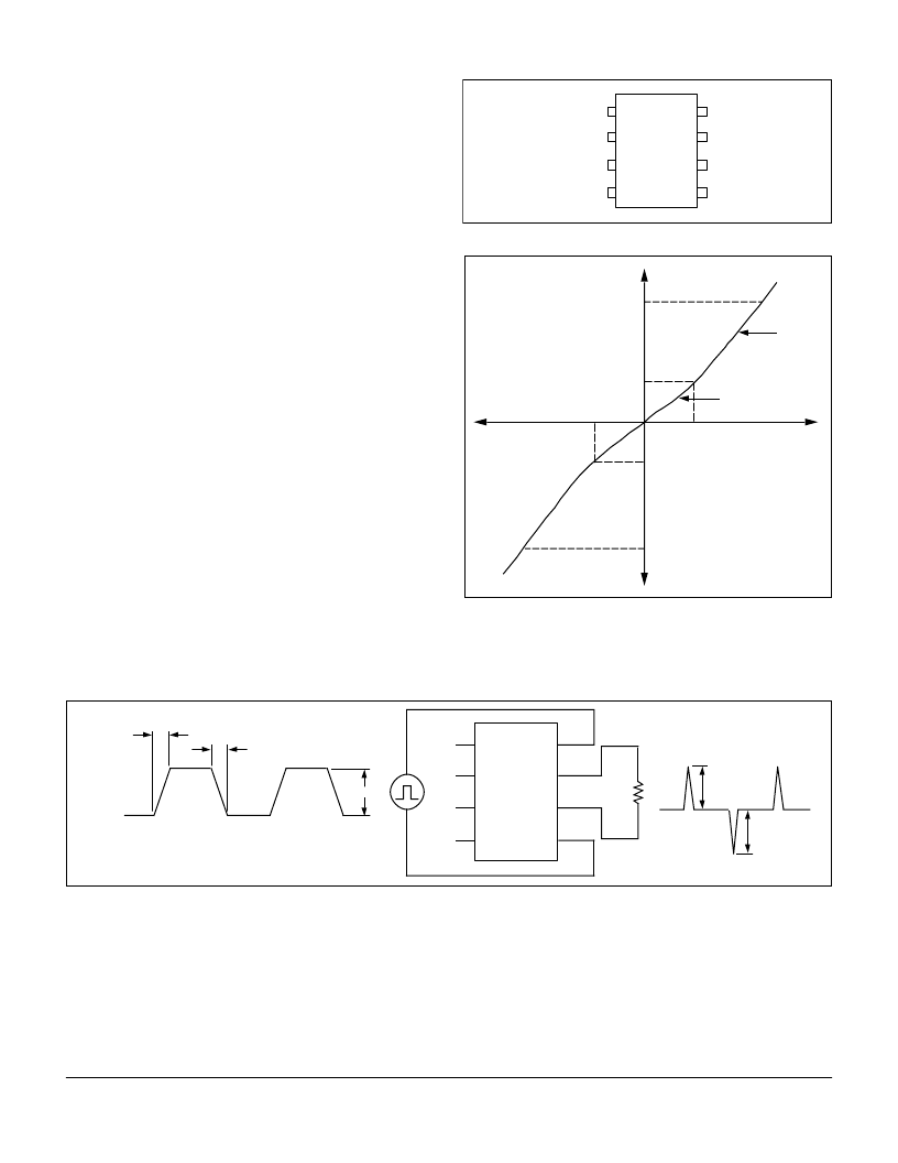
Functional Description
Figure 12 shows the switch characteristics of the relay. The
relay exhibits an ON-resistance that is exceptionally linear up
to the knee current (
I
K
). Beyond
I
K
, the incremental resistance
decreases, minimizing internal power dissipation.
In a 2 Form A relay, to turn the relay on, forward current is
applied to the LED. The amount of current applied determines
the amount of light produced for the photodiode array.
This photodiode array develops a drive voltage for both NMOS
switch outputs. For high-temperature or high-load current
operations, more LED current is required.
For high-frequency applications, the LH1514 must be wired as
shown in the Figure 15 application diagram to minimize trans-
mission crosstalk and bleed-through. A single LH1514 pack-
age switches a single transmit twisted pair or a single receive
twisted pair. In this configuration when the SSR is turned off,
the SSR parries high-frequency signals by shunting them
through the SSR, thereby isolating the transformer load.
When switching alternate mark inversion (AMI) coding trans-
mission, the most critical SSR parameter is dv/dt bleed-
through. This bleed-through is a result of the rise and fall time
slew rates of the 3.0 V AMI pulses. The test circuit in Figure 13
illustrates these bleed-through glitches. It is important to rec-
ognize that the transmission limitations of the LH1514 are
bleed-through related and not frequency related. The maxi-
mum frequency the LH1514 SSR can switch will be determined
by the pulse rise and fall times and the sensitivity of the receive
electronics to the resultant bleed-through.
At data rates above 2.0 Mbits/s, the 50 pF pole-to-pole capaci-
tance of the LH1514 should be considered when analyzing the
load match to the transmission line. Please refer to the
T1
Switching with the LH1514 SSR
Application Note for further
information on load-matching and off-state blocking.
Figure 11. Pin Diagram and Pin Outs
Figure 12. Typical ON Characteristics
1
2
3
S1
S1'
S2
CONTROL +
CONTROL +
CONTROL
–
8
7
6
DPST
4
S2'
BLANK
5
–
150 mA
150 mA
60 mA
–
60 mA
–
V
+V
+I
–
I
I
L
(max)
I
K
I
K
0.3 V
–
0.3 V
4.0
5.0
I
L
(max)
Test Circuit
Figure 13. Off-state Bleed-through
* 50
load is derived from T1 applications where a 100
load is paralleled with a 100
line.
NC
NC
NC
NC
1
2
3
4
8
7
6
5
100 mV
max
100 mV
max
50
*
tf 5.0 ns
f = 1.5 MHz
3.0 V
tr 5.0 ns
相關(guān)PDF資料 |
PDF描述 |
|---|---|
| LH1514AF | 80 OUTPUT LCD SEGMENT DRIVER |
| LH1514 | 80 OUTPUT LCD SEGMENT DRIVER |
| LH1516 | Conduit Cord Grip Connector; Cable Bundle Diameter Max:0.75"; Connector Shell Size:0.500 in; Hole Diameter:0.875" |
| LH1516A | HIGH VOLTAGE, PHOTO MOS RELAY |
| LH1518AAB | 1 Form A Solid State Relay |
相關(guān)代理商/技術(shù)參數(shù) |
參數(shù)描述 |
|---|---|
| LH1514AF | 制造商:SHARP 制造商全稱:Sharp Electrionic Components 功能描述:80 OUTPUT LCD SEGMENT DRIVER |
| LH1516 | 制造商:INFINEON 制造商全稱:Infineon Technologies AG 功能描述:High Voltage Solid State Relays |
| LH1516A | 制造商:未知廠家 制造商全稱:未知廠家 功能描述:HIGH VOLTAGE, PHOTO MOS RELAY |
| LH1516AAB | 制造商:未知廠家 制造商全稱:未知廠家 功能描述: |
| LH1516AT | 制造商:未知廠家 制造商全稱:未知廠家 功能描述: |
發(fā)布緊急采購,3分鐘左右您將得到回復(fù)。