- 您現(xiàn)在的位置:買賣IC網(wǎng) > PDF目錄377639 > LFX200B-4F900C (Lattice Semiconductor Corporation) The ispXPGA architecture PDF資料下載
參數(shù)資料
| 型號: | LFX200B-4F900C |
| 廠商: | Lattice Semiconductor Corporation |
| 英文描述: | The ispXPGA architecture |
| 中文描述: | 在ispXPGA架構(gòu) |
| 文件頁數(shù): | 12/89頁 |
| 文件大小: | 941K |
| 代理商: | LFX200B-4F900C |
第1頁第2頁第3頁第4頁第5頁第6頁第7頁第8頁第9頁第10頁第11頁當(dāng)前第12頁第13頁第14頁第15頁第16頁第17頁第18頁第19頁第20頁第21頁第22頁第23頁第24頁第25頁第26頁第27頁第28頁第29頁第30頁第31頁第32頁第33頁第34頁第35頁第36頁第37頁第38頁第39頁第40頁第41頁第42頁第43頁第44頁第45頁第46頁第47頁第48頁第49頁第50頁第51頁第52頁第53頁第54頁第55頁第56頁第57頁第58頁第59頁第60頁第61頁第62頁第63頁第64頁第65頁第66頁第67頁第68頁第69頁第70頁第71頁第72頁第73頁第74頁第75頁第76頁第77頁第78頁第79頁第80頁第81頁第82頁第83頁第84頁第85頁第86頁第87頁第88頁第89頁
Lattice Semiconductor
ispXPGA Family Data Sheet
12
Memory
The ispXPGA architecture provides a large amount of resources for memory intensive applications. Embedded
Block RAMs (EBRs) are available to complement the Distributed Memory that is con
fi
gured in the PFUs (see Look-
Up Table -Distributed Memory Mode in the PFU section above). Each memory element can be con
fi
gured as RAM
or ROM. Additionally, the internal logic of the device can be used to con
fi
gure the memory elements as FIFO and
other storage types. These EBRs are referred to as sysMEM blocks. Refer to Table 1 for memory resources per
device.
sysMEM Blocks
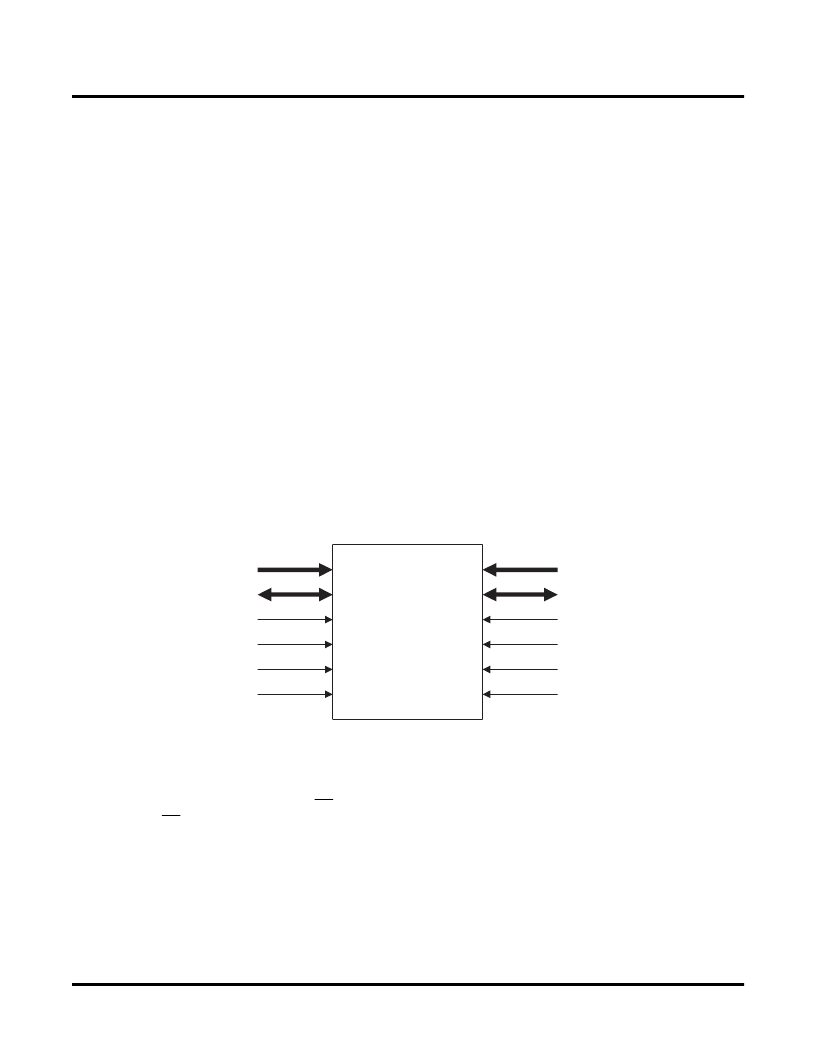
The sysMEM blocks are organized in columns distributed throughout the device. Each EBR contains 4.6K bits of
dual-port RAM with dedicated control, address, and data lines for each port. Each column of sysMEM blocks has
dedicated address and control lines that can be used by each block separately or cascaded to form larger memory
elements. The memory cells are symmetrical and contain two sets of identical control signals. Each port has a
read/write clock, clock enable, write enable, and output enable. Figure 12 illustrates the sysMEM block.
The ispXPGA memory block can operate as single-port or dual-port RAM. Supported con
fi
gurations are:
512 x 9 bits single-port
256 x 18 bits single-port
512 x 9 bits dual-port
256 x18 bits dual-port
(8 bits data / 1 bit parity)
(16 bits data / 2 bits parity)
(8 bits data / 1 bit parity)
(16 bits data / 2 bits parity)
The data widths of “9” and “18” are ideal for applications where parity is necessary. This allows 9 data bits, 8 data
bits plus a parity bit, 18 data bits, or 16 data bits plus two parity bits. The logic for generating and checking the par-
ity must be customized separately.
Figure 12. sysMEM Block Diagram
Read and Write Operations
The ispXPGA EBR has fully synchronous read and write operations as well as an asynchronous read operation.
These operations allow several different types of memory to be implemented in the device.
Synchronous Read:
tion. When the CE signal is low, the clock is enabled. When the WE signal is low the read operation begins. Once
the address (ADDR) is present, a rising clock edge (or falling edge depending on polarity) causes the stored data
to be available on the DATA port. Figure 13 illustrates the synchronous read timing.
The Clock Enable (CE) and Write Enable (WE) signals control the synchronous read opera-
sysMEM Block
ADDRA
DATAA
WEA
OEA
CLKA
CEA
ADDRB
DATAB
WEB
OEB
CLKB
CEB
相關(guān)PDF資料 |
PDF描述 |
|---|---|
| LFX500B-4F900C | The ispXPGA architecture |
| LFX1200B-4F900C | The ispXPGA architecture |
| LFX125C-4F900C | The ispXPGA architecture |
| LFX200C-4F900I | The ispXPGA architecture |
| LFX500B-3F900I | The ispXPGA architecture |
相關(guān)代理商/技術(shù)參數(shù) |
參數(shù)描述 |
|---|---|
| LFX200B-4F900I | 制造商:LATTICE 制造商全稱:Lattice Semiconductor 功能描述:ispXPGA Family |
| LFX200B-4FE680C | 制造商:LATTICE 制造商全稱:Lattice Semiconductor 功能描述:ispXPGA Family |
| LFX200B-4FE680I | 制造商:LATTICE 制造商全稱:Lattice Semiconductor 功能描述:ispXPGA Family |
| LFX200B-4FH516C | 制造商:LATTICE 制造商全稱:Lattice Semiconductor 功能描述:ispXPGA Family |
| LFX200B-4FH516I | 制造商:LATTICE 制造商全稱:Lattice Semiconductor 功能描述:ispXPGA Family |
發(fā)布緊急采購,3分鐘左右您將得到回復(fù)。