- 您現(xiàn)在的位置:買賣IC網(wǎng) > PDF目錄377640 > LFX125B-4F900I (Lattice Semiconductor Corporation) The ispXPGA architecture PDF資料下載
參數(shù)資料
| 型號: | LFX125B-4F900I |
| 廠商: | Lattice Semiconductor Corporation |
| 英文描述: | The ispXPGA architecture |
| 中文描述: | 在ispXPGA架構 |
| 文件頁數(shù): | 15/89頁 |
| 文件大小: | 941K |
| 代理商: | LFX125B-4F900I |
第1頁第2頁第3頁第4頁第5頁第6頁第7頁第8頁第9頁第10頁第11頁第12頁第13頁第14頁當前第15頁第16頁第17頁第18頁第19頁第20頁第21頁第22頁第23頁第24頁第25頁第26頁第27頁第28頁第29頁第30頁第31頁第32頁第33頁第34頁第35頁第36頁第37頁第38頁第39頁第40頁第41頁第42頁第43頁第44頁第45頁第46頁第47頁第48頁第49頁第50頁第51頁第52頁第53頁第54頁第55頁第56頁第57頁第58頁第59頁第60頁第61頁第62頁第63頁第64頁第65頁第66頁第67頁第68頁第69頁第70頁第71頁第72頁第73頁第74頁第75頁第76頁第77頁第78頁第79頁第80頁第81頁第82頁第83頁第84頁第85頁第86頁第87頁第88頁第89頁
Lattice Semiconductor
ispXPGA Family Data Sheet
15
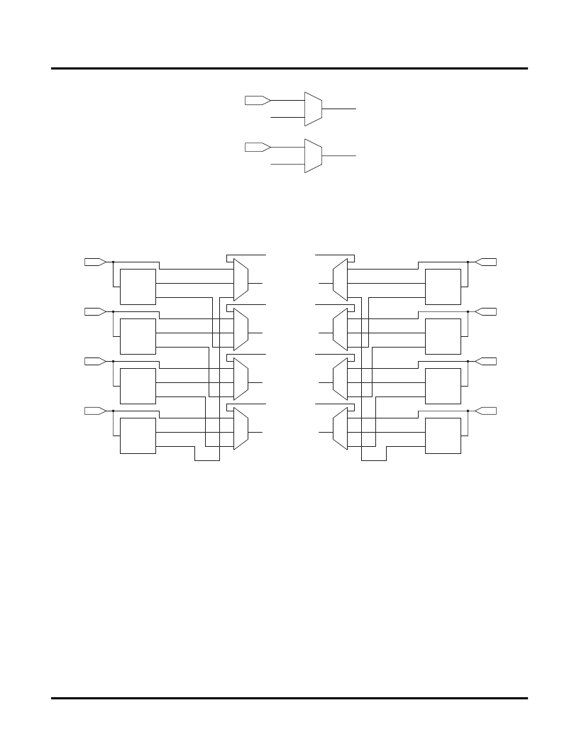
Figure 17. ispXPGA PLL_RST and PLL_FBK Generation
Clock Routing
The Global Clock Lines (GCLK) have two sources, their dedicated pins and the sysCLOCK circuit. Figure 18 illus-
trates the generation of the Global Clock Lines.
Figure 18. Global Clock Line Generation
sysIO Capability
All the ispXPGA devices have eight sysIO banks, where each bank is capable of supporting multiple I/O standards.
Each sysIO bank has its own I/O supply voltage (V
CCO
) and reference voltage (V
bank complete independence from the others. Each I/O is individually con
fi
gurable based on the bank’s V
V
REF
settings. In addition, each I/O has con
fi
gurable drive strength, weak pull-up, weak pull-down, or a bus-keeper
latch. Table 4 lists the number of I/Os supported per bank in each of the ispXPGA devices.
REF
) resources allowing each
CCO
and
Table 5 lists the sysIO standards with the typical values for V
CCO,
V
REF
and V
TT.
The TOE, JTAG TAP pins, PROGRAM, CFG0 and DONE pins of the ispXPGA device are the only pins that do not
have the sysIO capabilities. The TOE and CFG0 pins operate off the V
MOS standard corresponding to the device supply voltage. The TAP pins have a separate supply voltage (V
which determines the LVCMOS standard corresponding to that supply voltage.
CC
of the device, supporting only the LVC-
CCJ
),
There are three classes of I/O interface standards that are implemented in the ispXPGA devices. The
fi
rst is the un-
terminated, single-ended interface. It includes the 3.3V LVTTL standard along with the 1.8V, 2.5V, and 3.3V LVC-
MOS interface standards. Additionally, PCI and AGP-1X are subsets of this type of interface.
I/O/PLL_RST
I/O/PLL_FBK
From Routing
From Clock Net
To PLL
To PLL
PLL0
GCLK0
CLK_OUT0
SEC_OUT0
PLL1
CLK_OUT1
SEC_OUT1
GCLK1
PLL2
CLK_OUT2
SEC_OUT2
GCLK2
PLL3
CLK_OUT3
SEC_OUT3
GCLK3
PLL7
GCLK7
CLK_OUT7
SEC_OUT7
PLL6
CLK_OUT6
SEC_OUT6
GCLK6
PLL5
CLK_OUT5
SEC_OUT5
GCLK5
PLL4
CLK_OUT4
SEC_OUT4
GCLK4
CLK0
CLK1
CLK2
CLK3
CLK7
CLK6
CLK5
CLK4
From Routing
From Routing
From Routing
From Routing
相關PDF資料 |
PDF描述 |
|---|---|
| LFX200B-4F900I | The ispXPGA architecture |
| LFX500B-4F900I | The ispXPGA architecture |
| LG-205 | Photointerrupters(Transmissive) |
| LG-206 | Photointerrupters(Transmissive) |
| LG-209 | Photointerrupters(Transmissive) |
相關代理商/技術參數(shù) |
參數(shù)描述 |
|---|---|
| LFX125B-4FE680C | 制造商:LATTICE 制造商全稱:Lattice Semiconductor 功能描述:ispXPGA Family |
| LFX125B-4FE680I | 制造商:LATTICE 制造商全稱:Lattice Semiconductor 功能描述:ispXPGA Family |
| LFX125B-4FH516C | 制造商:LATTICE 制造商全稱:Lattice Semiconductor 功能描述:ispXPGA Family |
| LFX125B-4FH516I | 制造商:LATTICE 制造商全稱:Lattice Semiconductor 功能描述:ispXPGA Family |
| LFX125B-4FN256C | 制造商:LATTICE 制造商全稱:Lattice Semiconductor 功能描述:ispXPGA Family |
發(fā)布緊急采購,3分鐘左右您將得到回復。