- 您現(xiàn)在的位置:買賣IC網(wǎng) > PDF目錄377639 > LFX1200C-4F900C (Lattice Semiconductor Corporation) The ispXPGA architecture PDF資料下載
參數(shù)資料
| 型號(hào): | LFX1200C-4F900C |
| 廠商: | Lattice Semiconductor Corporation |
| 英文描述: | The ispXPGA architecture |
| 中文描述: | 在ispXPGA架構(gòu) |
| 文件頁數(shù): | 4/89頁 |
| 文件大小: | 941K |
| 代理商: | LFX1200C-4F900C |
第1頁第2頁第3頁當(dāng)前第4頁第5頁第6頁第7頁第8頁第9頁第10頁第11頁第12頁第13頁第14頁第15頁第16頁第17頁第18頁第19頁第20頁第21頁第22頁第23頁第24頁第25頁第26頁第27頁第28頁第29頁第30頁第31頁第32頁第33頁第34頁第35頁第36頁第37頁第38頁第39頁第40頁第41頁第42頁第43頁第44頁第45頁第46頁第47頁第48頁第49頁第50頁第51頁第52頁第53頁第54頁第55頁第56頁第57頁第58頁第59頁第60頁第61頁第62頁第63頁第64頁第65頁第66頁第67頁第68頁第69頁第70頁第71頁第72頁第73頁第74頁第75頁第76頁第77頁第78頁第79頁第80頁第81頁第82頁第83頁第84頁第85頁第86頁第87頁第88頁第89頁
Lattice Semiconductor
ispXPGA Family Data Sheet
4
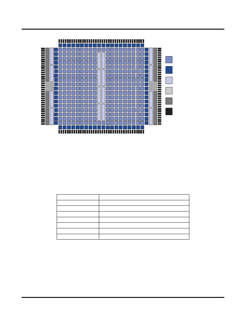
Figure 1. ispXPGA Block Diagram
Programmable Function Unit
The Programmable Function Unit (PFU) is the basic building block of the ispXPGA architecture. The PFUs are
arranged in rows and columns in the device with PFU (1,1) referring to (row 1, column 1). Each PFU consists of
four Con
fi
gurable Logic Elements (CLEs), four Con
fi
gurable Sequential Elements (CSEs), and a Wide Logic Gen-
erator (WLG). By utilizing these components, the PFU can implement a variety of functions. Table 3 lists some of
the function capabilities of the PFU.
There are 57 inputs to each PFU and nine outputs. The PFU uses 20 inputs for logic, and 37 inputs drive the con-
trol logic from which six control signals are derived for the PFU.
Table 3. Function Capability of ispXPGA PFU
Function
Capability
Look-up table
LUT-4, LUT-5, LUT-6
Wide logic functions
Up to 20 input logic functions
Multiplexing
2:1, 4:1, 8:1
Arithmetic logic
Dedicated carry chain and booth multiplication logic
Single-port RAM
16X1, 16X2, 16X4, 32X1, 32X2, 64X1
Double-port RAM
16X1, 16X2, 32X1
Shift register
8-bit shift registers (up to 32-bit shift capability)
PFU
PIC
sysHSI Block
sysCLOCK PLL
sysIO Buffer
sysMEM Block
相關(guān)PDF資料 |
PDF描述 |
|---|---|
| LFX125B-4F900C | The ispXPGA architecture |
| LFX200B-4F900C | The ispXPGA architecture |
| LFX500B-4F900C | The ispXPGA architecture |
| LFX1200B-4F900C | The ispXPGA architecture |
| LFX125C-4F900C | The ispXPGA architecture |
相關(guān)代理商/技術(shù)參數(shù) |
參數(shù)描述 |
|---|---|
| LFX1200C-4F900I | 制造商:LATTICE 制造商全稱:Lattice Semiconductor 功能描述:ispXPGA Family |
| LFX1200C-4FE680C | 制造商:LATTICE 制造商全稱:Lattice Semiconductor 功能描述:ispXPGA Family |
| LFX1200C-4FE680I | 制造商:LATTICE 制造商全稱:Lattice Semiconductor 功能描述:ispXPGA Family |
| LFX1200C-4FH516C | 制造商:LATTICE 制造商全稱:Lattice Semiconductor 功能描述:ispXPGA Family |
| LFX1200C-4FH516I | 制造商:LATTICE 制造商全稱:Lattice Semiconductor 功能描述:ispXPGA Family |
發(fā)布緊急采購,3分鐘左右您將得到回復(fù)。