- 您現(xiàn)在的位置:買賣IC網(wǎng) > PDF目錄377635 > LFECP1E-3F672I (Lattice Semiconductor Corporation) LatticeECP/EC Family Data Sheet PDF資料下載
參數(shù)資料
| 型號: | LFECP1E-3F672I |
| 廠商: | Lattice Semiconductor Corporation |
| 英文描述: | LatticeECP/EC Family Data Sheet |
| 中文描述: | LatticeECP / EC的系列數(shù)據(jù)手冊 |
| 文件頁數(shù): | 29/117頁 |
| 文件大小: | 557K |
| 代理商: | LFECP1E-3F672I |
第1頁第2頁第3頁第4頁第5頁第6頁第7頁第8頁第9頁第10頁第11頁第12頁第13頁第14頁第15頁第16頁第17頁第18頁第19頁第20頁第21頁第22頁第23頁第24頁第25頁第26頁第27頁第28頁當前第29頁第30頁第31頁第32頁第33頁第34頁第35頁第36頁第37頁第38頁第39頁第40頁第41頁第42頁第43頁第44頁第45頁第46頁第47頁第48頁第49頁第50頁第51頁第52頁第53頁第54頁第55頁第56頁第57頁第58頁第59頁第60頁第61頁第62頁第63頁第64頁第65頁第66頁第67頁第68頁第69頁第70頁第71頁第72頁第73頁第74頁第75頁第76頁第77頁第78頁第79頁第80頁第81頁第82頁第83頁第84頁第85頁第86頁第87頁第88頁第89頁第90頁第91頁第92頁第93頁第94頁第95頁第96頁第97頁第98頁第99頁第100頁第101頁第102頁第103頁第104頁第105頁第106頁第107頁第108頁第109頁第110頁第111頁第112頁第113頁第114頁第115頁第116頁第117頁
2-26
Architecture
Lattice Semiconductor
LatticeECP/EC Family Data Sheet
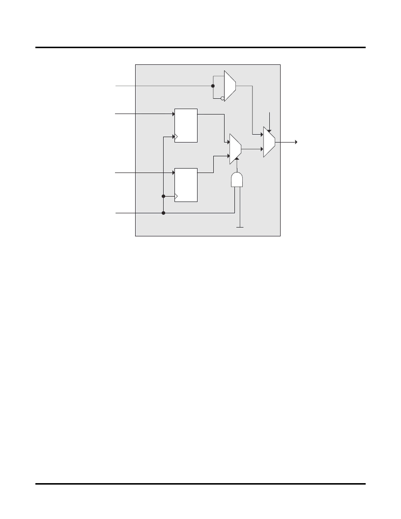
Figure 2-30. Tristate Register Block
Control Logic Block
The control logic block allows the selection and modi
fi
cation of control signals for use in the PIO block. A clock is
selected from one of the clock signals provided from the general purpose routing and a DQS signal provided from
the programmable DQS pin. The clock can optionally be inverted.
The clock enable and local reset signals are selected from the routing and optionally inverted. The global tristate
signal is passed through this block.
DDR Memory Support
Implementing high performance DDR memory interfaces requires dedicated DDR register structures in the input
(for read operations) and in the output (for write operations). As indicated in the PIO Logic section, the EC devices
provide this capability. In addition to these registers, the EC devices contain two elements to simplify the design of
input structures for read operations: the DQS delay block and polarity control logic.
DLL Calibrated DQS Delay Block
Source Synchronous interfaces generally require the input clock to be adjusted in order to correctly capture data at
the input register. For most interfaces a PLL is used for this adjustment, however in DDR memories the clock
(referred to as DQS) is not free running so this approach cannot be used. The DQS Delay block provides the
required clock alignment for DDR memory interfaces.
The DQS signal (selected PIOs only) feeds from the PAD through a DQS delay element to a dedicated DQS rout-
ing resource. The DQS signal also feeds polarity control logic which controls the polarity of the clock to the sync
registers in the input register blocks. Figures 2-31 and 2-32 show how the DQS transition signals are routed to the
PIOs.
The temperature, voltage and process variations of the DQS delay block are compensated by a set of calibration
(6-bit bus) signals from two DLLs on opposite sides of the device. Each DLL compensates DQS Delays in its half of
the device as shown in Figure 2-32. The DLL loop is compensated for temperature, voltage and process variations
by the system clock and feedback loop.
D
LE*
Q
D
D-Type
/LATCH
Q
ONEG1
CLK1
Programmed
Control
TO
Latch
*Latch is transparent when input is low.
OPOS1
OUTDDN
0
1
0
1
From
Routing
To sysIO
Buffer
TD
相關PDF資料 |
PDF描述 |
|---|---|
| LFEC3E-3F672I | LatticeECP/EC Family Data Sheet |
| LFECP3E-3F672I | LatticeECP/EC Family Data Sheet |
| LFEC6E-3F672I | LatticeECP/EC Family Data Sheet |
| LFECP6E-3F672I | LatticeECP/EC Family Data Sheet |
| LFEC10E-3F672I | LatticeECP/EC Family Data Sheet |
相關代理商/技術參數(shù) |
參數(shù)描述 |
|---|---|
| LFECP1E-3F900C | 制造商:LATTICE 制造商全稱:Lattice Semiconductor 功能描述:LatticeECP/EC Family Data Sheet |
| LFECP1E-3F900I | 制造商:LATTICE 制造商全稱:Lattice Semiconductor 功能描述:LatticeECP/EC Family Data Sheet |
| LFECP1E-3Q208C | 制造商:LATTICE 制造商全稱:Lattice Semiconductor 功能描述:LatticeECP/EC Family Data Sheet |
| LFECP1E-3Q208I | 制造商:LATTICE 制造商全稱:Lattice Semiconductor 功能描述:LatticeECP/EC Family Data Sheet |
| LFECP1E-3T100C | 制造商:LATTICE 制造商全稱:Lattice Semiconductor 功能描述:LatticeECP/EC Family Data Sheet |
發(fā)布緊急采購,3分鐘左右您將得到回復。