- 您現在的位置:買賣IC網 > PDF目錄377634 > LFECP15E-5T144C (Lattice Semiconductor Corporation) Enhanced Product 12-Bit Analog-To-Digital Converter W/ Serial Control And 11 Analog Input 20-SOIC -40 to 125 PDF資料下載
參數資料
| 型號: | LFECP15E-5T144C |
| 廠商: | Lattice Semiconductor Corporation |
| 英文描述: | Enhanced Product 12-Bit Analog-To-Digital Converter W/ Serial Control And 11 Analog Input 20-SOIC -40 to 125 |
| 中文描述: | LatticeECP / EC的系列數據手冊 |
| 文件頁數: | 8/117頁 |
| 文件大小: | 557K |
| 代理商: | LFECP15E-5T144C |
第1頁第2頁第3頁第4頁第5頁第6頁第7頁當前第8頁第9頁第10頁第11頁第12頁第13頁第14頁第15頁第16頁第17頁第18頁第19頁第20頁第21頁第22頁第23頁第24頁第25頁第26頁第27頁第28頁第29頁第30頁第31頁第32頁第33頁第34頁第35頁第36頁第37頁第38頁第39頁第40頁第41頁第42頁第43頁第44頁第45頁第46頁第47頁第48頁第49頁第50頁第51頁第52頁第53頁第54頁第55頁第56頁第57頁第58頁第59頁第60頁第61頁第62頁第63頁第64頁第65頁第66頁第67頁第68頁第69頁第70頁第71頁第72頁第73頁第74頁第75頁第76頁第77頁第78頁第79頁第80頁第81頁第82頁第83頁第84頁第85頁第86頁第87頁第88頁第89頁第90頁第91頁第92頁第93頁第94頁第95頁第96頁第97頁第98頁第99頁第100頁第101頁第102頁第103頁第104頁第105頁第106頁第107頁第108頁第109頁第110頁第111頁第112頁第113頁第114頁第115頁第116頁第117頁
2-5
Architecture
Lattice Semiconductor
LatticeECP/EC Family Data Sheet
Modes of Operation
Each Slice is capable of four modes of operation: Logic, Ripple, RAM and ROM. The Slice in the PFF is capable of
all modes except RAM. Table 2-2 lists the modes and the capability of the Slice blocks.
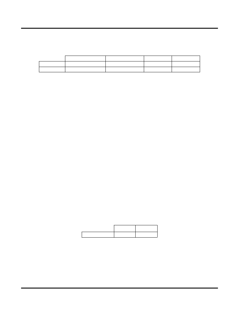
Table 2-2. Slice Modes
Logic Mode:
can have 16 possible input combinations. Any logic function with four inputs can be generated by programming this
lookup table. Since there are two LUT4s per Slice, a LUT5 can be constructed within one Slice. Larger lookup
tables such as LUT6, LUT7 and LUT8 can be constructed by concatenating other Slices.
In this mode, the LUTs in each Slice are con
fi
gured as 4-input combinatorial lookup tables. A LUT4
Ripple Mode:
lowing functions can be implemented by each Slice:
Ripple mode allows the ef
fi
cient implementation of small arithmetic functions. In ripple mode, the fol-
Addition 2-bit
Subtraction 2-bit
Add/Subtract 2-bit using dynamic control
Up counter 2-bit
Down counter 2-bit
Ripple mode multiplier building block
Comparator functions of A and B inputs
- A greater-than-or-equal-to B
- A not-equal-to B
- A less-than-or-equal-to B
Two additional signals: Carry Generate and Carry Propagate are generated per Slice in this mode, allowing fast
arithmetic functions to be constructed by concatenating Slices.
RAM Mode:
Through the combination of LUTs and Slices, a variety of different memories can be constructed.
In this mode, distributed RAM can be constructed using each LUT block as a 16x1-bit memory.
The Lattice design tools support the creation of a variety of different size memories. Where appropriate, the soft-
ware will construct these using distributed memory primitives that represent the capabilities of the PFU. Table 2-3
shows the number of Slices required to implement different distributed RAM primitives. Figure 2-5 shows the dis-
tributed memory primitive block diagrams. Dual port memories involve the pairing of two Slices, one Slice functions
as the read-write port. The other companion Slice supports the read-only port. For more information on using RAM
in LatticeECP/EC devices, please see details of additional technical documentation at the end of this data sheet.
Table 2-3. Number of Slices Required For Implementing Distributed RAM
Logic
Ripple
RAM
SPR16x2
N/A
ROM
PFU Slice
PFF Slice
LUT 4x2 or LUT 5x1
LUT 4x2 or LUT 5x1
2-bit Arithmetic Unit
2-bit Arithmetic Unit
ROM16x1 x 2
ROM16x1 x 2
SPR16x2
1
DPR16x2
2
Number of slices
Note: SPR = Single Port RAM, DPR = Dual Port RAM
相關PDF資料 |
PDF描述 |
|---|---|
| LFECP15E-5T144I | Enhanced Product 12-Bit Analog-To-Digital Converter W/ Serial Control And 11 Analog Input 20-SSOP -55 to 125 |
| LFECP1E-5F484C | Automotive Catalog 12-Bit Analog-to-Digital Converters With Serial Control and 11 Analog Inputs 20-SSOP -40 to 85 |
| LFECP1E-5F484I | Automotive Catalog 12-Bit Analog-to-Digital Converters With Serial Control and 11 Analog Inputs 20-SSOP -40 to 85 |
| LFECP1E-5T100C | LatticeECP/EC Family Data Sheet |
| LFECP1E-5T100I | LatticeECP/EC Family Data Sheet |
相關代理商/技術參數 |
參數描述 |
|---|---|
| LFECP15E-5T144I | 制造商:LATTICE 制造商全稱:Lattice Semiconductor 功能描述:LatticeECP/EC Family Data Sheet |
| LFECP15E-5TN100C | 制造商:LATTICE 制造商全稱:Lattice Semiconductor 功能描述:LatticeECP/EC Family Data Sheet |
| LFECP15E-5TN100I | 制造商:LATTICE 制造商全稱:Lattice Semiconductor 功能描述:LatticeECP/EC Family Data Sheet |
| LFECP15E-5TN144C | 制造商:LATTICE 制造商全稱:Lattice Semiconductor 功能描述:LatticeECP/EC Family Data Sheet |
| LFECP15E-5TN144I | 制造商:LATTICE 制造商全稱:Lattice Semiconductor 功能描述:LatticeECP/EC Family Data Sheet |
發(fā)布緊急采購,3分鐘左右您將得到回復。