- 您現(xiàn)在的位置:買賣IC網(wǎng) > PDF目錄377636 > LFECP10E-3F900C (Lattice Semiconductor Corporation) LatticeECP/EC Family Data Sheet PDF資料下載
參數(shù)資料
| 型號(hào): | LFECP10E-3F900C |
| 廠商: | Lattice Semiconductor Corporation |
| 英文描述: | LatticeECP/EC Family Data Sheet |
| 中文描述: | LatticeECP / EC的系列數(shù)據(jù)手冊(cè) |
| 文件頁數(shù): | 36/117頁 |
| 文件大小: | 557K |
| 代理商: | LFECP10E-3F900C |
第1頁第2頁第3頁第4頁第5頁第6頁第7頁第8頁第9頁第10頁第11頁第12頁第13頁第14頁第15頁第16頁第17頁第18頁第19頁第20頁第21頁第22頁第23頁第24頁第25頁第26頁第27頁第28頁第29頁第30頁第31頁第32頁第33頁第34頁第35頁當(dāng)前第36頁第37頁第38頁第39頁第40頁第41頁第42頁第43頁第44頁第45頁第46頁第47頁第48頁第49頁第50頁第51頁第52頁第53頁第54頁第55頁第56頁第57頁第58頁第59頁第60頁第61頁第62頁第63頁第64頁第65頁第66頁第67頁第68頁第69頁第70頁第71頁第72頁第73頁第74頁第75頁第76頁第77頁第78頁第79頁第80頁第81頁第82頁第83頁第84頁第85頁第86頁第87頁第88頁第89頁第90頁第91頁第92頁第93頁第94頁第95頁第96頁第97頁第98頁第99頁第100頁第101頁第102頁第103頁第104頁第105頁第106頁第107頁第108頁第109頁第110頁第111頁第112頁第113頁第114頁第115頁第116頁第117頁
2-33
Architecture
Lattice Semiconductor
LatticeECP/EC Family Data Sheet
Oscillator
Every LatticeECP/EC device has an internal CMOS oscillator which is used to derive a master serial clock for con-
fi
guration. The oscillator and the master serial clock run continuously. The default value of the master serial clock is
2.5MHz. Table 2-15 lists all the available Master Serial Clock frequencies. When a different Master Serial Clock is
selected during the design process, the following sequence takes place:
1.
User selects a different Master Serial Clock frequency.
2.
During con
fi
guration the device starts with the default (2.5MHz) Master Serial Clock frequency.
3.
The clock con
fi
guration settings are contained in the early con
fi
guration bit stream.
4.
The Master Serial Clock frequency changes to the selected frequency once the clock con
fi
guration bits are
received.
For further information on the use of this oscillator for con
fi
guration, please see details of additional technical docu-
mentation at the end of this data sheet.
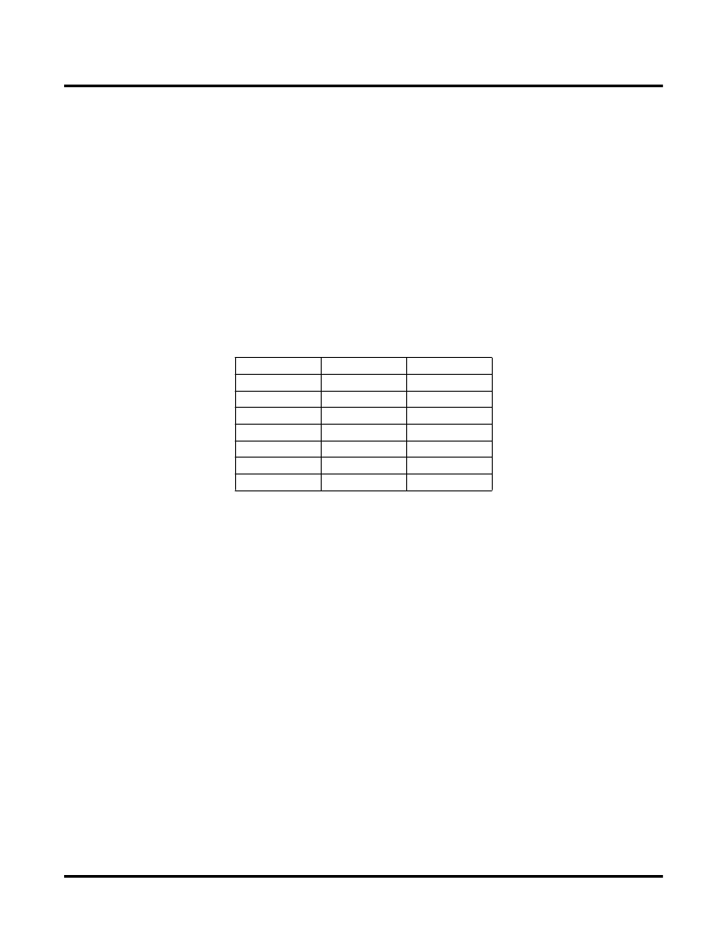
Table 2-15. Selectable Master Serial Clock (CCLK) Frequencies During Configuration
Density Shifting
The LatticeECP/EC family has been designed to ensure that different density devices in the same package have
the same pin-out. Furthermore, the architecture ensures a high success rate when performing design migration
from lower density parts to higher density parts. In many cases, it is also possible to shift a lower utilization design
targeted for a high-density device to a lower density device. However, the exact details of the
fi
nal resource utiliza-
tion will impact the likely success in each case.
CCLK (MHz)
2.5*
4.3
5.4
6.9
8.1
9.2
10.0
CCLK (MHz)
13
15
20
26
30
34
41
CCLK (MHz)
45
51
55
60
130
—
—
相關(guān)PDF資料 |
PDF描述 |
|---|---|
| LFEC15E-3F900C | LatticeECP/EC Family Data Sheet |
| LFECP15E-3F900C | LatticeECP/EC Family Data Sheet |
| LFEC20E-3F900C | LatticeECP/EC Family Data Sheet |
| LFECP20E-3F900C | LatticeECP/EC Family Data Sheet |
| LFEC40E-3F900C | LatticeECP/EC Family Data Sheet |
相關(guān)代理商/技術(shù)參數(shù) |
參數(shù)描述 |
|---|---|
| LFECP10E-3F900I | 制造商:LATTICE 制造商全稱:Lattice Semiconductor 功能描述:LatticeECP/EC Family Data Sheet |
| LFECP10E-3FN256C | 功能描述:FPGA - 現(xiàn)場(chǎng)可編程門陣列 10.2K LUTs Pb-Free RoHS:否 制造商:Altera Corporation 系列:Cyclone V E 柵極數(shù)量: 邏輯塊數(shù)量:943 內(nèi)嵌式塊RAM - EBR:1956 kbit 輸入/輸出端數(shù)量:128 最大工作頻率:800 MHz 工作電源電壓:1.1 V 最大工作溫度:+ 70 C 安裝風(fēng)格:SMD/SMT 封裝 / 箱體:FBGA-256 |
| LFECP10E-3FN256I | 功能描述:FPGA - 現(xiàn)場(chǎng)可編程門陣列 10.2K LUTs 195 I/O RoHS:否 制造商:Altera Corporation 系列:Cyclone V E 柵極數(shù)量: 邏輯塊數(shù)量:943 內(nèi)嵌式塊RAM - EBR:1956 kbit 輸入/輸出端數(shù)量:128 最大工作頻率:800 MHz 工作電源電壓:1.1 V 最大工作溫度:+ 70 C 安裝風(fēng)格:SMD/SMT 封裝 / 箱體:FBGA-256 |
| LFECP10E-3FN484C | 功能描述:FPGA - 現(xiàn)場(chǎng)可編程門陣列 10.2K LUTs Pb-Free RoHS:否 制造商:Altera Corporation 系列:Cyclone V E 柵極數(shù)量: 邏輯塊數(shù)量:943 內(nèi)嵌式塊RAM - EBR:1956 kbit 輸入/輸出端數(shù)量:128 最大工作頻率:800 MHz 工作電源電壓:1.1 V 最大工作溫度:+ 70 C 安裝風(fēng)格:SMD/SMT 封裝 / 箱體:FBGA-256 |
| LFECP10E-3FN484I | 功能描述:FPGA - 現(xiàn)場(chǎng)可編程門陣列 10.2K LUTs 288 I/O RoHS:否 制造商:Altera Corporation 系列:Cyclone V E 柵極數(shù)量: 邏輯塊數(shù)量:943 內(nèi)嵌式塊RAM - EBR:1956 kbit 輸入/輸出端數(shù)量:128 最大工作頻率:800 MHz 工作電源電壓:1.1 V 最大工作溫度:+ 70 C 安裝風(fēng)格:SMD/SMT 封裝 / 箱體:FBGA-256 |
發(fā)布緊急采購(gòu),3分鐘左右您將得到回復(fù)。