- 您現(xiàn)在的位置:買賣IC網(wǎng) > PDF目錄377639 > LFEC3E-4F672C (Lattice Semiconductor Corporation) LatticeECP/EC Family Data Sheet PDF資料下載
參數(shù)資料
| 型號(hào): | LFEC3E-4F672C |
| 廠商: | Lattice Semiconductor Corporation |
| 英文描述: | LatticeECP/EC Family Data Sheet |
| 中文描述: | LatticeECP / EC的系列數(shù)據(jù)手冊(cè) |
| 文件頁(yè)數(shù): | 14/117頁(yè) |
| 文件大小: | 557K |
| 代理商: | LFEC3E-4F672C |
第1頁(yè)第2頁(yè)第3頁(yè)第4頁(yè)第5頁(yè)第6頁(yè)第7頁(yè)第8頁(yè)第9頁(yè)第10頁(yè)第11頁(yè)第12頁(yè)第13頁(yè)當(dāng)前第14頁(yè)第15頁(yè)第16頁(yè)第17頁(yè)第18頁(yè)第19頁(yè)第20頁(yè)第21頁(yè)第22頁(yè)第23頁(yè)第24頁(yè)第25頁(yè)第26頁(yè)第27頁(yè)第28頁(yè)第29頁(yè)第30頁(yè)第31頁(yè)第32頁(yè)第33頁(yè)第34頁(yè)第35頁(yè)第36頁(yè)第37頁(yè)第38頁(yè)第39頁(yè)第40頁(yè)第41頁(yè)第42頁(yè)第43頁(yè)第44頁(yè)第45頁(yè)第46頁(yè)第47頁(yè)第48頁(yè)第49頁(yè)第50頁(yè)第51頁(yè)第52頁(yè)第53頁(yè)第54頁(yè)第55頁(yè)第56頁(yè)第57頁(yè)第58頁(yè)第59頁(yè)第60頁(yè)第61頁(yè)第62頁(yè)第63頁(yè)第64頁(yè)第65頁(yè)第66頁(yè)第67頁(yè)第68頁(yè)第69頁(yè)第70頁(yè)第71頁(yè)第72頁(yè)第73頁(yè)第74頁(yè)第75頁(yè)第76頁(yè)第77頁(yè)第78頁(yè)第79頁(yè)第80頁(yè)第81頁(yè)第82頁(yè)第83頁(yè)第84頁(yè)第85頁(yè)第86頁(yè)第87頁(yè)第88頁(yè)第89頁(yè)第90頁(yè)第91頁(yè)第92頁(yè)第93頁(yè)第94頁(yè)第95頁(yè)第96頁(yè)第97頁(yè)第98頁(yè)第99頁(yè)第100頁(yè)第101頁(yè)第102頁(yè)第103頁(yè)第104頁(yè)第105頁(yè)第106頁(yè)第107頁(yè)第108頁(yè)第109頁(yè)第110頁(yè)第111頁(yè)第112頁(yè)第113頁(yè)第114頁(yè)第115頁(yè)第116頁(yè)第117頁(yè)
2-11
Architecture
Lattice Semiconductor
LatticeECP/EC Family Data Sheet
Table 2-5. PLL Signal Descriptions
For more information on the PLL, please see details of additional technical documentation at the end of this data
sheet.
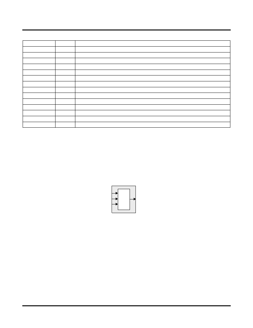
Dynamic Clock Select (DCS)
The DCS is a global clock buffer with smart multiplexer functions. It takes two independent input clock sources and
outputs a clock signal without any glitches or runt pulses. This is achieved irrespective of where the select signal is
toggled. There are eight DCS blocks per device, located in pairs at the center of each side. Figure 2-13 illustrates
the DCS Block Macro.
Figure 2-13. DCS Block Primitive
Figure 2-14 shows timing waveforms of the default DCS operating mode. The DCS block can be programmed to
other modes. For more information on the DCS, please see details of additional technical documentation at the end
of this data sheet.
Signal
I/O
I
I
I
O
O
O
O
I
I
I
I
O
O
O
Description
CLKI
CLKFB
RST
CLKOS
CLKOP
CLKOK
LOCK
DDAMODE
DDAIZR
DDAILAG
DDAIDEL[2:0]
DDAOZR
DDAOLAG
DDAODEL[2:0]
Clock input from external pin or routing
PLL feedback input from CLKOP, clocknet, or external pin
“1” to reset PLL
PLL output clock to clock tree (phase shifted/duty cycle changed)
PLL output clock to clock tree (No phase shift)
PLL output to clock tree through secondary clock divider
“1” indicates PLL LOCK to CLKI
Dynamic Delay Enable. “1”: Pin control (dynamic), “0”: Fuse Control (static)
Dynamic Delay Zero. “1”: delay = 0, “0”: delay = on
Dynamic Delay Lag/Lead. “1”: Lead, “0”: Lag
Dynamic Delay Input
Dynamic Delay Zero Output
Dynamic Delay Lag/Lead Output
Dynamic Delay Output
DCS
CLK0
DCSOUT
CLK1
SEL
相關(guān)PDF資料 |
PDF描述 |
|---|---|
| LFEC3E-4F672I | LatticeECP/EC Family Data Sheet |
| LFEC3E-4F900I | LatticeECP/EC Family Data Sheet |
| LFEC3E-4T100I | LatticeECP/EC Family Data Sheet |
| LFEC3E-4T144C | LatticeECP/EC Family Data Sheet |
| LFEC3E-4T144I | LatticeECP/EC Family Data Sheet |
相關(guān)代理商/技術(shù)參數(shù) |
參數(shù)描述 |
|---|---|
| LFEC3E-4F672I | 制造商:LATTICE 制造商全稱:Lattice Semiconductor 功能描述:LatticeECP/EC Family Data Sheet |
| LFEC3E-4F900C | 制造商:LATTICE 制造商全稱:Lattice Semiconductor 功能描述:LatticeECP/EC Family Data Sheet |
| LFEC3E-4F900I | 制造商:LATTICE 制造商全稱:Lattice Semiconductor 功能描述:LatticeECP/EC Family Data Sheet |
| LFEC3E-4FN256C | 功能描述:FPGA - 現(xiàn)場(chǎng)可編程門陣列 3.1K LUTs Pb-Free RoHS:否 制造商:Altera Corporation 系列:Cyclone V E 柵極數(shù)量: 邏輯塊數(shù)量:943 內(nèi)嵌式塊RAM - EBR:1956 kbit 輸入/輸出端數(shù)量:128 最大工作頻率:800 MHz 工作電源電壓:1.1 V 最大工作溫度:+ 70 C 安裝風(fēng)格:SMD/SMT 封裝 / 箱體:FBGA-256 |
| LFEC3E-4FN256I | 功能描述:FPGA - 現(xiàn)場(chǎng)可編程門陣列 3.1K LUTs 1.2V -4 Sp d I RoHS:否 制造商:Altera Corporation 系列:Cyclone V E 柵極數(shù)量: 邏輯塊數(shù)量:943 內(nèi)嵌式塊RAM - EBR:1956 kbit 輸入/輸出端數(shù)量:128 最大工作頻率:800 MHz 工作電源電壓:1.1 V 最大工作溫度:+ 70 C 安裝風(fēng)格:SMD/SMT 封裝 / 箱體:FBGA-256 |
發(fā)布緊急采購(gòu),3分鐘左右您將得到回復(fù)。