- 您現(xiàn)在的位置:買賣IC網(wǎng) > PDF目錄377639 > LFEC3E-4F256C (LATTICE SEMICONDUCTOR CORP) LatticeECP/EC Family Data Sheet PDF資料下載
參數(shù)資料
| 型號(hào): | LFEC3E-4F256C |
| 廠商: | LATTICE SEMICONDUCTOR CORP |
| 元件分類: | FPGA |
| 英文描述: | LatticeECP/EC Family Data Sheet |
| 中文描述: | FPGA, 384 CLBS, 3100 GATES, 420 MHz, PBGA256 |
| 封裝: | 17 X 17 MM, FPBGA-256 |
| 文件頁數(shù): | 15/117頁 |
| 文件大小: | 557K |
| 代理商: | LFEC3E-4F256C |
第1頁第2頁第3頁第4頁第5頁第6頁第7頁第8頁第9頁第10頁第11頁第12頁第13頁第14頁當(dāng)前第15頁第16頁第17頁第18頁第19頁第20頁第21頁第22頁第23頁第24頁第25頁第26頁第27頁第28頁第29頁第30頁第31頁第32頁第33頁第34頁第35頁第36頁第37頁第38頁第39頁第40頁第41頁第42頁第43頁第44頁第45頁第46頁第47頁第48頁第49頁第50頁第51頁第52頁第53頁第54頁第55頁第56頁第57頁第58頁第59頁第60頁第61頁第62頁第63頁第64頁第65頁第66頁第67頁第68頁第69頁第70頁第71頁第72頁第73頁第74頁第75頁第76頁第77頁第78頁第79頁第80頁第81頁第82頁第83頁第84頁第85頁第86頁第87頁第88頁第89頁第90頁第91頁第92頁第93頁第94頁第95頁第96頁第97頁第98頁第99頁第100頁第101頁第102頁第103頁第104頁第105頁第106頁第107頁第108頁第109頁第110頁第111頁第112頁第113頁第114頁第115頁第116頁第117頁
2-12
Architecture
Lattice Semiconductor
LatticeECP/EC Family Data Sheet
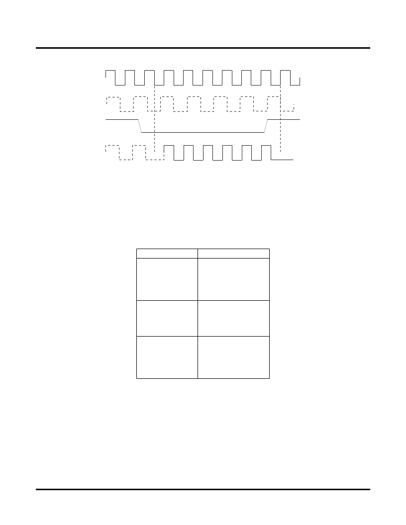
Figure 2-14. DCS Waveforms
sysMEM Memory
The LatticeECP/EC family of devices contain a number of sysMEM Embedded Block RAM (EBR). The EBR con-
sists of a 9-Kbit RAM, with dedicated input and output registers.
sysMEM Memory Block
The sysMEM block can implement single port, dual port or pseudo dual port memories. Each block can be used in
a variety of depths and widths as shown in Table 2-6.
Table 2-6. sysMEM Block Configurations
Bus Size Matching
All of the multi-port memory modes support different widths on each of the ports. The RAM bits are mapped LSB
word 0 to MSB word 0, LSB word 1 to MSB word 1 and so on. Although the word size and number of words for
each port varies, this mapping scheme applies to each port.
RAM Initialization and ROM Operation
If desired, the contents of the RAM can be pre-loaded during device con
fi
guration. By preloading the RAM block
during the chip con
fi
guration cycle and disabling the write controls, the sysMEM block can also be utilized as a
ROM.
Memory Mode
Con
fi
gurations
8,192 x 1
4,096 x 2
2,048 x 4
1,024 x 9
512 x 18
256 x 36
8,192 x 1
4,096 x 2
2,048 x 4
1,024 x 9
512 x 18
8,192 x 1
4,096 x 2
2,048 x 4
1,024 x 9
512 x 18
256 x 36
Single Port
True Dual Port
Pseudo Dual Port
CLK0
SEL
DCSOUT
CLK1
相關(guān)PDF資料 |
PDF描述 |
|---|---|
| LFEC3E-4F256I | LatticeECP/EC Family Data Sheet |
| LFEC3E-4F484C | LatticeECP/EC Family Data Sheet |
| LFEC3E-4F484I | LatticeECP/EC Family Data Sheet |
| LFEC3E-4F672C | LatticeECP/EC Family Data Sheet |
| LFEC3E-4F672I | LatticeECP/EC Family Data Sheet |
相關(guān)代理商/技術(shù)參數(shù) |
參數(shù)描述 |
|---|---|
| LFEC3E-4F256CES | 功能描述:FPGA - 現(xiàn)場可編程門陣列 3.1 LUT 160 I/O RoHS:否 制造商:Altera Corporation 系列:Cyclone V E 柵極數(shù)量: 邏輯塊數(shù)量:943 內(nèi)嵌式塊RAM - EBR:1956 kbit 輸入/輸出端數(shù)量:128 最大工作頻率:800 MHz 工作電源電壓:1.1 V 最大工作溫度:+ 70 C 安裝風(fēng)格:SMD/SMT 封裝 / 箱體:FBGA-256 |
| LFEC3E-4F256I | 功能描述:FPGA - 現(xiàn)場可編程門陣列 3.1K LUTs 1.2V -4 Sp d I RoHS:否 制造商:Altera Corporation 系列:Cyclone V E 柵極數(shù)量: 邏輯塊數(shù)量:943 內(nèi)嵌式塊RAM - EBR:1956 kbit 輸入/輸出端數(shù)量:128 最大工作頻率:800 MHz 工作電源電壓:1.1 V 最大工作溫度:+ 70 C 安裝風(fēng)格:SMD/SMT 封裝 / 箱體:FBGA-256 |
| LFEC3E-4F256IES | 功能描述:FPGA - 現(xiàn)場可編程門陣列 3.1 LUT 160 I/O RoHS:否 制造商:Altera Corporation 系列:Cyclone V E 柵極數(shù)量: 邏輯塊數(shù)量:943 內(nèi)嵌式塊RAM - EBR:1956 kbit 輸入/輸出端數(shù)量:128 最大工作頻率:800 MHz 工作電源電壓:1.1 V 最大工作溫度:+ 70 C 安裝風(fēng)格:SMD/SMT 封裝 / 箱體:FBGA-256 |
| LFEC3E-4F484C | 制造商:LATTICE 制造商全稱:Lattice Semiconductor 功能描述:LatticeECP/EC Family Data Sheet |
| LFEC3E-4F484I | 制造商:LATTICE 制造商全稱:Lattice Semiconductor 功能描述:LatticeECP/EC Family Data Sheet |
發(fā)布緊急采購,3分鐘左右您將得到回復(fù)。