- 您現(xiàn)在的位置:買賣IC網(wǎng) > PDF目錄377631 > LFEC33E-4F484C (LATTICE SEMICONDUCTOR CORP) LatticeECP/EC Family Data Sheet PDF資料下載
參數(shù)資料
| 型號: | LFEC33E-4F484C |
| 廠商: | LATTICE SEMICONDUCTOR CORP |
| 元件分類: | FPGA |
| 英文描述: | LatticeECP/EC Family Data Sheet |
| 中文描述: | FPGA, 4096 CLBS, 32800 GATES, 420 MHz, PBGA484 |
| 封裝: | 23 X 23 MM, FPBGA-484 |
| 文件頁數(shù): | 12/117頁 |
| 文件大?。?/td> | 557K |
| 代理商: | LFEC33E-4F484C |
第1頁第2頁第3頁第4頁第5頁第6頁第7頁第8頁第9頁第10頁第11頁當(dāng)前第12頁第13頁第14頁第15頁第16頁第17頁第18頁第19頁第20頁第21頁第22頁第23頁第24頁第25頁第26頁第27頁第28頁第29頁第30頁第31頁第32頁第33頁第34頁第35頁第36頁第37頁第38頁第39頁第40頁第41頁第42頁第43頁第44頁第45頁第46頁第47頁第48頁第49頁第50頁第51頁第52頁第53頁第54頁第55頁第56頁第57頁第58頁第59頁第60頁第61頁第62頁第63頁第64頁第65頁第66頁第67頁第68頁第69頁第70頁第71頁第72頁第73頁第74頁第75頁第76頁第77頁第78頁第79頁第80頁第81頁第82頁第83頁第84頁第85頁第86頁第87頁第88頁第89頁第90頁第91頁第92頁第93頁第94頁第95頁第96頁第97頁第98頁第99頁第100頁第101頁第102頁第103頁第104頁第105頁第106頁第107頁第108頁第109頁第110頁第111頁第112頁第113頁第114頁第115頁第116頁第117頁
2-9
Architecture
Lattice Semiconductor
LatticeECP/EC Family Data Sheet
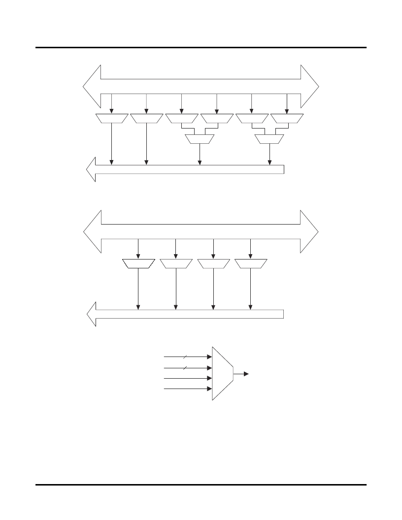
Figure 2-8. Per Quadrant Primary Clock Selection
Figure 2-9. Per Quadrant Secondary Clock Selection
Figure 2-10. Slice Clock Selection
sysCLOCK Phase Locked Loops (PLLs)
The PLL clock input, from pin or routing, feeds into an input clock divider. There are three sources of feedback sig-
nal to the feedback divider: from the CLKOP, from the clock net, or from an external pin. There is a PLL_LOCK sig-
nal to indicate that VCO has locked on to the input clock signal. Figure 2-11 shows the sysCLOCK PLL diagram.
The setup and hold times of the device can be improved by programming a delay in the feedback or input path of
the PLL which will advance or delay the output clock with reference to the input clock. This delay can be either pro-
grammed during con
fi
guration or can be adjusted dynamically. In dynamic mode, the PLL may lose lock after
4 Primary Clocks (CLK0, CLK1, CLK2, CLK3) per Quadrant
20 Primary Clock Sources: 12 PLLs + 4 PIOs + 4 Routing
1
DCS
DCS
1. Smaller devices have fewer PLL related lines.
4 Secondary Clocks per Quadrant
20 Secondary Clock Feedlines : 4 Clock Input Pads + 16 Routing Signals
Primary Clock
Secondary Clock
Routing
Clock to Slice
GND
4
3
相關(guān)PDF資料 |
PDF描述 |
|---|---|
| LFEC33E-4F484I | LatticeECP/EC Family Data Sheet |
| LFEC33E-4F672C | ECONOLINE: RSZ/P - 1kVDC |
| LFEC33E-4F672I | LatticeECP/EC Family Data Sheet |
| LFEC33E-4F900I | ECONOLINE: RSZ/P - 1kVDC |
| LFEC33E-4Q208I | LatticeECP/EC Family Data Sheet |
相關(guān)代理商/技術(shù)參數(shù) |
參數(shù)描述 |
|---|---|
| LFEC33E-4F484I | 功能描述:FPGA - 現(xiàn)場可編程門陣列 32.8K LUTs 360 I/O RoHS:否 制造商:Altera Corporation 系列:Cyclone V E 柵極數(shù)量: 邏輯塊數(shù)量:943 內(nèi)嵌式塊RAM - EBR:1956 kbit 輸入/輸出端數(shù)量:128 最大工作頻率:800 MHz 工作電源電壓:1.1 V 最大工作溫度:+ 70 C 安裝風(fēng)格:SMD/SMT 封裝 / 箱體:FBGA-256 |
| LFEC33E-4F672C | 功能描述:FPGA - 現(xiàn)場可編程門陣列 32.8K LUTs RoHS:否 制造商:Altera Corporation 系列:Cyclone V E 柵極數(shù)量: 邏輯塊數(shù)量:943 內(nèi)嵌式塊RAM - EBR:1956 kbit 輸入/輸出端數(shù)量:128 最大工作頻率:800 MHz 工作電源電壓:1.1 V 最大工作溫度:+ 70 C 安裝風(fēng)格:SMD/SMT 封裝 / 箱體:FBGA-256 |
| LFEC33E-4F672I | 功能描述:FPGA - 現(xiàn)場可編程門陣列 32.8K LUTs 496 I/O RoHS:否 制造商:Altera Corporation 系列:Cyclone V E 柵極數(shù)量: 邏輯塊數(shù)量:943 內(nèi)嵌式塊RAM - EBR:1956 kbit 輸入/輸出端數(shù)量:128 最大工作頻率:800 MHz 工作電源電壓:1.1 V 最大工作溫度:+ 70 C 安裝風(fēng)格:SMD/SMT 封裝 / 箱體:FBGA-256 |
| LFEC33E-4F900C | 制造商:LATTICE 制造商全稱:Lattice Semiconductor 功能描述:LatticeECP/EC Family Data Sheet |
| LFEC33E-4F900I | 制造商:LATTICE 制造商全稱:Lattice Semiconductor 功能描述:LatticeECP/EC Family Data Sheet |
發(fā)布緊急采購,3分鐘左右您將得到回復(fù)。