- 您現(xiàn)在的位置:買賣IC網(wǎng) > PDF目錄377633 > LFEC15E-4T144C (Lattice Semiconductor Corporation) LatticeECP/EC Family Data Sheet PDF資料下載
參數(shù)資料
| 型號: | LFEC15E-4T144C |
| 廠商: | Lattice Semiconductor Corporation |
| 英文描述: | LatticeECP/EC Family Data Sheet |
| 中文描述: | LatticeECP / EC的系列數(shù)據(jù)手冊 |
| 文件頁數(shù): | 32/117頁 |
| 文件大?。?/td> | 557K |
| 代理商: | LFEC15E-4T144C |
第1頁第2頁第3頁第4頁第5頁第6頁第7頁第8頁第9頁第10頁第11頁第12頁第13頁第14頁第15頁第16頁第17頁第18頁第19頁第20頁第21頁第22頁第23頁第24頁第25頁第26頁第27頁第28頁第29頁第30頁第31頁當(dāng)前第32頁第33頁第34頁第35頁第36頁第37頁第38頁第39頁第40頁第41頁第42頁第43頁第44頁第45頁第46頁第47頁第48頁第49頁第50頁第51頁第52頁第53頁第54頁第55頁第56頁第57頁第58頁第59頁第60頁第61頁第62頁第63頁第64頁第65頁第66頁第67頁第68頁第69頁第70頁第71頁第72頁第73頁第74頁第75頁第76頁第77頁第78頁第79頁第80頁第81頁第82頁第83頁第84頁第85頁第86頁第87頁第88頁第89頁第90頁第91頁第92頁第93頁第94頁第95頁第96頁第97頁第98頁第99頁第100頁第101頁第102頁第103頁第104頁第105頁第106頁第107頁第108頁第109頁第110頁第111頁第112頁第113頁第114頁第115頁第116頁第117頁
2-29
Architecture
Lattice Semiconductor
LatticeECP/EC Family Data Sheet
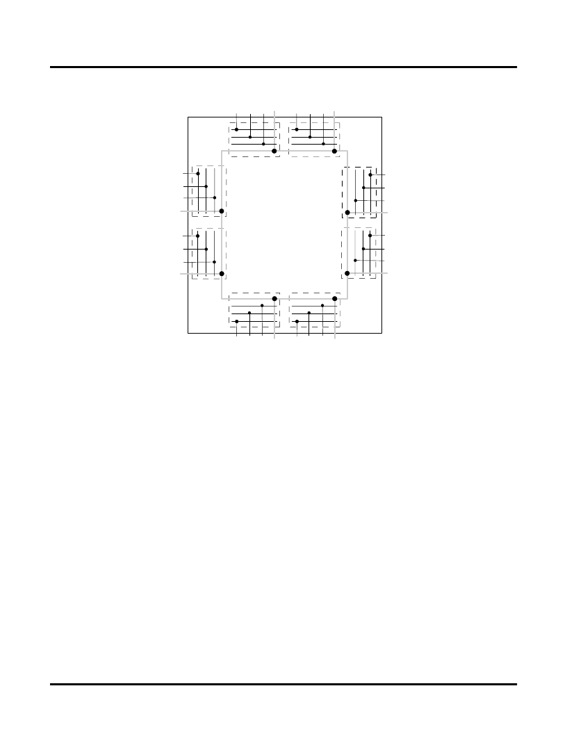
Figure 2-33. LatticeECP/EC Banks
LatticeECP/EC devices contain two types of sysIO buffer pairs.
1.
Top and Bottom sysIO Buffer Pair (Single-Ended Outputs Only)
The sysIO buffer pairs in the top and bottom banks of the device consist of two single-ended output drivers and
two sets of single-ended input buffers (both ratioed and referenced). The referenced input buffer can also be
con
fi
gured as a differential input.
The two pads in the pair are described as “true” and “comp”, where the true pad is associated with the positive
side of the differential input buffer and the comp (complementary) pad is associated with the negative side of
the differential input buffer.
Only the I/Os on the top and bottom banks have PCI clamp.
2.
Left and Right sysIO Buffer Pair (Differential and Single-Ended Outputs)
The sysIO buffer pairs in the left and right banks of the device consist of two single-ended output drivers, two
sets of single-ended input buffers (both ratioed and referenced) and one differential output driver. The refer-
enced input buffer can also be con
fi
gured as a differential input. In these banks the two pads in the pair are
described as “true” and “comp”, where the true pad is associated with the positive side of the differential I/O,
and the comp (complementary) pad is associated with the negative side of the differential I/O.
Only the left and right banks have LVDS differential output drivers.
Supported Standards
The LatticeECP/EC sysIO buffer supports both single-ended and differential standards. Single-ended standards
can be further subdivided into LVCMOS, LVTTL and other standards. The buffers support the LVTTL, LVCMOS 1.2,
1.5, 1.8, 2.5 and 3.3V standards. In the LVCMOS and LVTTL modes, the buffer has individually con
fi
gurable
V
REF1(2)
V
REF2(2)
GND
B
V
CCIO2
V
REF1(3)
V
REF2(3)
GND
B
V
CCIO3
V
REF1(7)
V
REF2(7)
GND
B
V
CCIO7
V
REF1(6)
V
REF2(6)
GND
Note: N and M are the maximum number of I/Os per bank.
B
V
CCIO6
V
R
G
Bank 5
V
C
V
R
V
R
G
Bank 4
V
C
V
R
V
R
G
Bank 0
V
C
V
R
V
R
G
Bank 1
V
C
V
R
M
相關(guān)PDF資料 |
PDF描述 |
|---|---|
| LFEC15E-4T144I | LatticeECP/EC Family Data Sheet |
| LFEC15E-5F256C | LatticeECP/EC Family Data Sheet |
| LFEC15E-5F256I | LatticeECP/EC Family Data Sheet |
| LFEC15E-5F484C | LatticeECP/EC Family Data Sheet |
| LFEC15E-5F484I | LatticeECP/EC Family Data Sheet |
相關(guān)代理商/技術(shù)參數(shù) |
參數(shù)描述 |
|---|---|
| LFEC15E-4T144I | 制造商:LATTICE 制造商全稱:Lattice Semiconductor 功能描述:LatticeECP/EC Family Data Sheet |
| LFEC15E-4TN100C | 制造商:LATTICE 制造商全稱:Lattice Semiconductor 功能描述:LatticeECP/EC Family Data Sheet |
| LFEC15E-4TN100I | 制造商:LATTICE 制造商全稱:Lattice Semiconductor 功能描述:LatticeECP/EC Family Data Sheet |
| LFEC15E-4TN144C | 制造商:LATTICE 制造商全稱:Lattice Semiconductor 功能描述:LatticeECP/EC Family Data Sheet |
| LFEC15E-4TN144I | 制造商:LATTICE 制造商全稱:Lattice Semiconductor 功能描述:LatticeECP/EC Family Data Sheet |
發(fā)布緊急采購,3分鐘左右您將得到回復(fù)。