- 您現(xiàn)在的位置:買賣IC網(wǎng) > PDF目錄377632 > LFEC15E-3T144C (Lattice Semiconductor Corporation) LatticeECP/EC Family Data Sheet PDF資料下載
參數(shù)資料
| 型號: | LFEC15E-3T144C |
| 廠商: | Lattice Semiconductor Corporation |
| 英文描述: | LatticeECP/EC Family Data Sheet |
| 中文描述: | LatticeECP / EC的系列數(shù)據(jù)手冊 |
| 文件頁數(shù): | 24/117頁 |
| 文件大?。?/td> | 557K |
| 代理商: | LFEC15E-3T144C |
第1頁第2頁第3頁第4頁第5頁第6頁第7頁第8頁第9頁第10頁第11頁第12頁第13頁第14頁第15頁第16頁第17頁第18頁第19頁第20頁第21頁第22頁第23頁當前第24頁第25頁第26頁第27頁第28頁第29頁第30頁第31頁第32頁第33頁第34頁第35頁第36頁第37頁第38頁第39頁第40頁第41頁第42頁第43頁第44頁第45頁第46頁第47頁第48頁第49頁第50頁第51頁第52頁第53頁第54頁第55頁第56頁第57頁第58頁第59頁第60頁第61頁第62頁第63頁第64頁第65頁第66頁第67頁第68頁第69頁第70頁第71頁第72頁第73頁第74頁第75頁第76頁第77頁第78頁第79頁第80頁第81頁第82頁第83頁第84頁第85頁第86頁第87頁第88頁第89頁第90頁第91頁第92頁第93頁第94頁第95頁第96頁第97頁第98頁第99頁第100頁第101頁第102頁第103頁第104頁第105頁第106頁第107頁第108頁第109頁第110頁第111頁第112頁第113頁第114頁第115頁第116頁第117頁
2-21
Architecture
Lattice Semiconductor
LatticeECP/EC Family Data Sheet
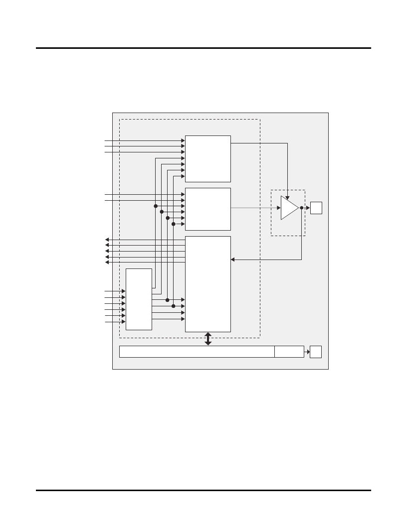
Programmable I/O Cells (PIC)
Each PIC contains two PIOs connected to their respective sysIO Buffers which are then connected to the PADs as
shown in Figure 2-23. The PIO Block supplies the output data (DO) and the Tri-state control signal (TO) to sysIO
buffer, and receives input from the buffer.
Figure 2-23. PIC Diagram
Two adjacent PIOs can be joined to provide a differential I/O pair (labeled as “T” and “C”) as shown in Figure 2-24.
The PAD Labels “T” and “C” distinguish the two PIOs. Only the PIO pairs on the left and right edges of the device
can be con
fi
gured as LVDS transmit/receive pairs.
One of every 16 PIOs contains a delay element to facilitate the generation of DQS signals. The DQS signal feeds
the DQS bus which spans the set of 16 PIOs. Figure 2-24 shows the assignment of DQS pins in each set of 16
PIOs. The exact DQS pins are shown in a dual function in the Logic Signal Connections table at the end of this data
sheet. Additional detail is provided in the Signal Descriptions table at the end of this data sheet. The DQS signal
from the bus is used to strobe the DDR data from the memory into input register blocks. This interface is designed
for memories that support one DQS strobe per eight bits of data.
PIO B
PADA
"T"
PADB
"C"
OPOS0
ONEG0
OPOS1
ONEG1
TD
INCK
INDD
INFF
IPOS0
IPOS1
CLK
CE
LSR
GSRN
DQS
PIO A
sysIO
Buffer
DDRCLKPOL
IOLD0
IOLT0
D0
D1
DDRCLK
DI
IPOS1
IPOS0
INCK
INDD
INFF
D0
D1
DDRCLK
TD
Output
Register Block
(2 Flip Flops)
Tristate
Register Block
(2 Flip Flops)
Input
Register Block
(5 Flip Flops)
CLKO
CEO
LSR
GSR
CLKI
CEI
Control
Muxes
相關(guān)PDF資料 |
PDF描述 |
|---|---|
| LFEC15E-3T144I | LatticeECP/EC Family Data Sheet |
| LFEC15E-4F256C | LatticeECP/EC Family Data Sheet |
| LFEC15E-4F484C | LatticeECP/EC Family Data Sheet |
| LFEC15E-4F484I | LatticeECP/EC Family Data Sheet |
| LFEC15E-4F672C | LatticeECP/EC Family Data Sheet |
相關(guān)代理商/技術(shù)參數(shù) |
參數(shù)描述 |
|---|---|
| LFEC15E-3T144I | 制造商:LATTICE 制造商全稱:Lattice Semiconductor 功能描述:LatticeECP/EC Family Data Sheet |
| LFEC15E-3TN100C | 制造商:LATTICE 制造商全稱:Lattice Semiconductor 功能描述:LatticeECP/EC Family Data Sheet |
| LFEC15E-3TN100I | 制造商:LATTICE 制造商全稱:Lattice Semiconductor 功能描述:LatticeECP/EC Family Data Sheet |
| LFEC15E-3TN144C | 制造商:LATTICE 制造商全稱:Lattice Semiconductor 功能描述:LatticeECP/EC Family Data Sheet |
| LFEC15E-3TN144I | 制造商:LATTICE 制造商全稱:Lattice Semiconductor 功能描述:LatticeECP/EC Family Data Sheet |
發(fā)布緊急采購,3分鐘左右您將得到回復。