- 您現(xiàn)在的位置:買賣IC網(wǎng) > PDF目錄377624 > LF3304QC12 (LOGIC DEVICES INC) Circular Connector; No. of Contacts:23; Series:; Body Material:Aluminum; Connecting Termination:Crimp; Connector Shell Size:16; Circular Contact Gender:Pin; Circular Shell Style:Box Mount Receptacle; Insert Arrangement:16-99 PDF資料下載
參數(shù)資料
| 型號: | LF3304QC12 |
| 廠商: | LOGIC DEVICES INC |
| 元件分類: | 存儲器 |
| 英文描述: | Circular Connector; No. of Contacts:23; Series:; Body Material:Aluminum; Connecting Termination:Crimp; Connector Shell Size:16; Circular Contact Gender:Pin; Circular Shell Style:Box Mount Receptacle; Insert Arrangement:16-99 |
| 中文描述: | SPECIALTY MEMORY CIRCUIT, PQFP100 |
| 封裝: | PLASTIC, QFP-100 |
| 文件頁數(shù): | 2/12頁 |
| 文件大小: | 130K |
| 代理商: | LF3304QC12 |
DEVICES INCORPORATED
LF3304
Dual Line Buffer/FIFO
2
Video Imaging Products
08/16/2000–LDS.3304-F
the data presented on LENGTH
11-0
is
loaded into the device on the active edge of
WCLKA in conjunction with LDA being
driven LOW. To set the length of RAM
Array B the data presented on
LENGTH
11-0
is loaded into the device
on the active edge of WCLKB in
conjunction with LDB being driven
LOW. If an equal length is desired for
both RAM Arrays, the data presented
on LENGTH
11-0
is loaded into the
device on the active edge of WCLK
(WCLKA and WCLKB tied together) in
conjuction with LDx (LDA and LDB
tied together) being driven LOW.
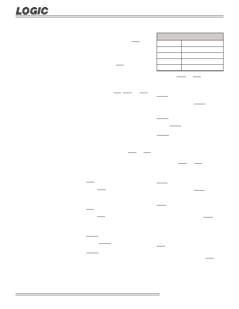
MODE
1-0
— Mode Select
The mode select inputs determine the
operating mode of the LF3304 (Table 1) for
data being input on the next clock cycle.
When switching between modes, the
internal pipeline latencies of the device
must be observed. After switching
operating modes, either the user must
allow enough clock clycles to pass to flush
the internal RAM Array or RWx and RRx
must be driven LOW together before valid
data will appear on the outputs.
Controls
LDA — RAM Array A Load
When LDA is LOW, data on
LENGTH
11-0
is latched in the length
register on the rising edge of xCLKA.
LDB — RAM Array B Load
When LDB is LOW, data on
LENGTH
11-0
is latched in the length
register on the rising edge of xCLKB.
WENA — Write Enable A
Driving WENA LOW places the device in
programmable delay mode and driving
WENA HIGH places RAM Array A in
recirculate mode (programmable circular
buffer). When in recirculate mode, the
write pointer position remains fixed while
data on AIN
11-0
is ignored. When
switching back from recirculate mode to
MODE
Mode Select
0 0
Dual Line Buffer
0 1
Cascaded Line Buffer
1 0
Dual FIFO
1 1
Reserved
delay mode, RWA and RRA should be
brought LOW to properly reset the Write
and Read pointers.
RENA — Read Enable B
In Line Buffer mode, RENA must be
kept LOW.
WENB — Write Enable B
Driving WENB LOW places the device in
programmable delay mode and driving
WENB HIGH places RAM Array B in
recirculate mode (programmable circular
buffer). When in recirculate mode, the
write pointer position remains fixed
while data on BIN
11-0
is ignored. When
switching back from recirculate mode to
delay mode, RWB and RRB should be
brought LOW to properly reset the Write
and Read pointers.
RENB — Read Enable B
In Line Buffer mode, RENB must be
kept LOW.
RWA — Reset Write A
The write address pointer is reset to the
first physical location when RWA is set
LOW. After power up, the LF3304
requires a Reset Write for initialization
because the write address pointer is not
defined at that time.
RRA — Reset Read A
The read address pointer is reset to the
first physical location when RRA is set
LOW. After power up, the LF3304
requires a Reset Read for initialization
because the read address pointer is not
defined at that time.
LINE BUFFER MODE
SIGNAL DEFINITIONS
Power
V
CC
and GND
+3.3 V power supply. All pins must
be connected.
Clocks
WCLKA — Write Clock A
WCLKA and RCLKA must be tied
together for RAM Array A to properly
operate as a Line Buffer. The rising edge
of xCLKA strobes all appropriate
enabled registers.
RCLKA — Read Clock A
See WCLKA description.
WCLKB — Write Clock B
WCLKB and RCLKB must be tied
together for RAM Array B to properly
operate as a Line Buffer. The rising
edge of xCLKB strobes all appropriate
enabled registers.
RCLKB — Read Clock B
See WCLKB description.
Inputs
AIN
11-0
— Data Input
A
AIN
11-0
is the 12-bit registered data
input port.
BIN
11-0
— Data Input
B
BIN
11-0
is the 12-bit registered data
input port.
LENGTH
11-0
— Line Buffer Length
The 12-bit value is used to specify the
length of each of the RAM Arrays. An
integer value ranging from 0 to 4095 is
used to select a delay ranging from 2 to
4097 clock cycles. The value placed on
LENGTH
11-0
is equal to the desired delay
minus 8. To set the length of RAM Array A
T
ABLE
1.
D
EVICE
C
ONFIGURATION
相關(guān)PDF資料 |
PDF描述 |
|---|---|
| LF3304QC15 | Circular Connector; Body Material:Aluminum; Series:PT02; No. of Contacts:23; Connector Shell Size:16; Connecting Termination:Crimp; Circular Shell Style:Box Mount Receptacle; Circular Contact Gender:Socket; Insert Arrangement:16-99 |
| LF3320 | Horizontal Digital Image Filter(水平數(shù)字圖像濾波器) |
| LF3320QC12 | Horizontal Digital Image Filter |
| LF3320QC15 | Horizontal Digital Image Filter |
| LF3330 | Vertical Digital Image Filter(垂直數(shù)字圖像濾波器) |
相關(guān)代理商/技術(shù)參數(shù) |
參數(shù)描述 |
|---|---|
| LF3304QC15 | 制造商:LOGIC 制造商全稱:LOGIC 功能描述:Dual Line Buffer/FIFO |
| LF-330A | 制造商:NEC 制造商全稱:NEC 功能描述:Noise Filters |
| LF-330K4 | 制造商:NEC 制造商全稱:NEC 功能描述:Noise Filters |
| LF3310 | 制造商:LOGIC 制造商全稱:LOGIC 功能描述:Horizontal / Vertical Digital Image Filter |
| LF3310QC12 | 制造商:LOGIC 制造商全稱:LOGIC 功能描述:Horizontal / Vertical Digital Image Filter |
發(fā)布緊急采購,3分鐘左右您將得到回復(fù)。