- 您現(xiàn)在的位置:買賣IC網(wǎng) > PDF目錄377624 > LF3304QC10 (LOGIC DEVICES INC) Circular Connector; No. of Contacts:23; Series:; Body Material:Aluminum; Connecting Termination:Crimp; Connector Shell Size:16; Circular Contact Gender:Pin; Circular Shell Style:Box Mount Receptacle; Insert Arrangement:16-99 PDF資料下載
參數(shù)資料
| 型號: | LF3304QC10 |
| 廠商: | LOGIC DEVICES INC |
| 元件分類: | 存儲器 |
| 英文描述: | Circular Connector; No. of Contacts:23; Series:; Body Material:Aluminum; Connecting Termination:Crimp; Connector Shell Size:16; Circular Contact Gender:Pin; Circular Shell Style:Box Mount Receptacle; Insert Arrangement:16-99 |
| 中文描述: | SPECIALTY MEMORY CIRCUIT, PQFP100 |
| 封裝: | PLASTIC, QFP-100 |
| 文件頁數(shù): | 3/12頁 |
| 文件大?。?/td> | 130K |
| 代理商: | LF3304QC10 |
DEVICES INCORPORATED
Video Imaging Products
3
LF3304
Dual Line Buffer/FIFO
08/16/2000–LDS.3304-F
RWB — Reset Write B
See RWA Description.
RRB — Reset Read B
See RRA description.
OEA — Output Enable A
When OEA is LOW, AOUT
11-0
is
enabled for output. When OEA is
HIGH, AOUT
11-0
is placed in a high-
impedence state.
OEB — Output Enable B
When OEB is LOW, BOUT
11-0
is
enabled for output. When OEB is
HIGH, BOUT
11-0
is placed in a high-
impedence state.
Outputs
AOUT
11-0
— Data Output A
AOUT
11-0
is the 12-bit registered
data output port.
BOUT
11-0
— Data Output B
BOUT
11-0
is the 12-bit registered
data output port.
FIFO MODE
SIGNAL DEFINITIONS
Power
V
CC
and GND
+3.3 V power supply. All pins must be
connected.
Clocks
WCLKA — Write Clock A
Data present on AIN
11-0
is written
into the LF3304 on the rising edge of
WCLKA when the device is configured
for writing.
RCLKA — Read Clock A
Data is read from the LF3304 and
presented on the output port (AOUT
11-0
)
after
t
D
has elapsed from the rising
edge of RCLKA when the device is
configured for reading and the output
port is enabled. WCLKA and RCLKA
can be tied together and driven by the
same external clock or they may be
controlled by separate external clocks.
WCLKB — Write Clock B
Data present on BIN
11-0
is written into
the LF3304 on the rising edge of
WCLKB when the device is configured
for writing.
RCLKB — Read Clock B
Data is read from the LF3304 and
presented on the output port (BOUT
11-0
)
after
t
D
has elapsed from the rising
edge of RCLKB when the device is
configured for reading and the output
port is enabled. WCLKB and RCLKB
can be tied together and driven by the
same external clock or they may be
controlled by separate external clocks.
Inputs
AIN
11-0
— Data Input
A
AIN
11-0
is the 12-bit registered data
input port.
BIN
11-0
— Data Input
B
BIN
11-0
is the 12-bit registered data
input port.
ADDRA — Address A
If LDA is LOW, on the rising edge of
WCLKA data present on AIN
11-0
is
written into the PAFA or PAEA register
depending on ADDRA (see Table 2).
The LSB, AIN
0
, corresponds to the LSB
of PAFA and PAEA registers. The MSB,
AIN
11
, corresponds to the MSB of PAFA
and PAEA registers.
ADDRB — Address B
If LDB is LOW, on the rising edge of
WCLKB data present on BIN
11-0
is
written into the PAFB or PAEB register
depending on ADDRB (see Table 2).
The LSB, BIN
0
, corresponds to the LSB
of PAFB and PAEB registers. The MSB,
BIN
11
, corresponds to the MSB of PAFB
and PAEB registers.
MODE
1-0
— Mode Select
The mode select inputs determine the
operating mode of the LF3304 (Table 1) for
data being input on the next clock cycle.
When switching between modes, the
internal pipeline latencies of the device
must be observed. After switching
operating modes, either the user must
allow enough clock clycles to pass to flush
the internal RAM Array or RWx and RRx
must be driven LOW together before valid
data will appear on the outputs.
LENGTH — Non-Flag Pins
In FIFO Mode, the unused LENGTH pins
(LENGTH
11
, LENGTH
10
, LENGTH
5
,
LENGTH
4
) must be tied LOW.
Controls
LDA — RAM Array A Load
When LDA is LOW, data on AIN
11-0
is
latched in the LF3304 on the rising edge
of WCLKA.
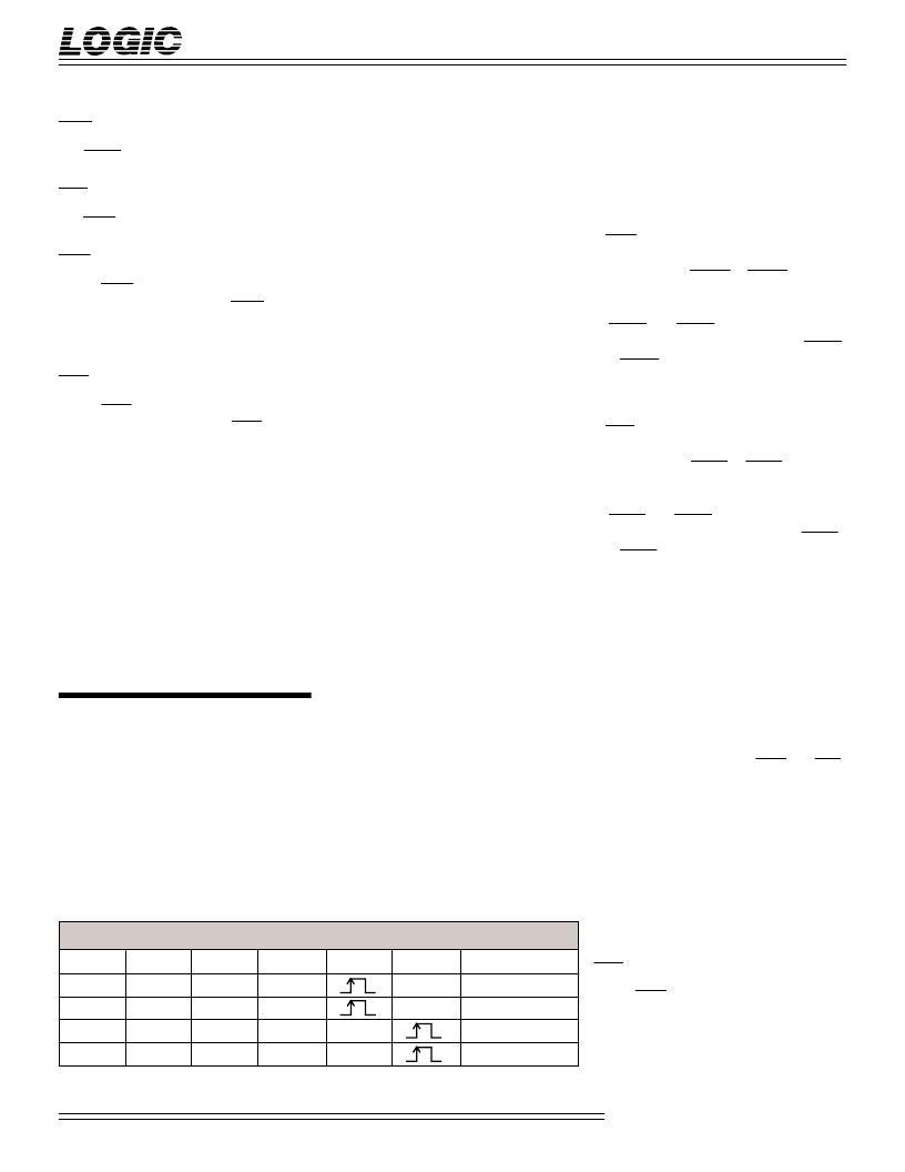
T
ABLE
2.
L
OADING
P
ROGRAMMABLE
F
LAG
R
EGISTERS
ADDRA
ADDRB
LDA
LDB
WCLKA
WCLKB
Operation
0
x
0
x
x
PAEA Register
1
x
0
x
x
PAFA Register
x
0
x
0
x
PAEB Register
x
1
x
0
x
PAFB Register
相關PDF資料 |
PDF描述 |
|---|---|
| LF3304QC12 | Circular Connector; No. of Contacts:23; Series:; Body Material:Aluminum; Connecting Termination:Crimp; Connector Shell Size:16; Circular Contact Gender:Pin; Circular Shell Style:Box Mount Receptacle; Insert Arrangement:16-99 |
| LF3304QC15 | Circular Connector; Body Material:Aluminum; Series:PT02; No. of Contacts:23; Connector Shell Size:16; Connecting Termination:Crimp; Circular Shell Style:Box Mount Receptacle; Circular Contact Gender:Socket; Insert Arrangement:16-99 |
| LF3320 | Horizontal Digital Image Filter(水平數(shù)字圖像濾波器) |
| LF3320QC12 | Horizontal Digital Image Filter |
| LF3320QC15 | Horizontal Digital Image Filter |
相關代理商/技術參數(shù) |
參數(shù)描述 |
|---|---|
| LF3304QC12 | 制造商:LOGIC 制造商全稱:LOGIC 功能描述:Dual Line Buffer/FIFO |
| LF3304QC15 | 制造商:LOGIC 制造商全稱:LOGIC 功能描述:Dual Line Buffer/FIFO |
| LF-330A | 制造商:NEC 制造商全稱:NEC 功能描述:Noise Filters |
| LF-330K4 | 制造商:NEC 制造商全稱:NEC 功能描述:Noise Filters |
| LF3310 | 制造商:LOGIC 制造商全稱:LOGIC 功能描述:Horizontal / Vertical Digital Image Filter |
發(fā)布緊急采購,3分鐘左右您將得到回復。