- 您現(xiàn)在的位置:買賣IC網(wǎng) > PDF目錄383278 > LF257 (意法半導(dǎo)體) Wide Bandwidth Single J-FET Operational Amplifiers(寬帶J-FET單運放) PDF資料下載
參數(shù)資料
| 型號: | LF257 |
| 廠商: | 意法半導(dǎo)體 |
| 英文描述: | Wide Bandwidth Single J-FET Operational Amplifiers(寬帶J-FET單運放) |
| 中文描述: | 寬帶單的J - FET的運算放大器(寬帶的J - FET的單運放) |
| 文件頁數(shù): | 4/14頁 |
| 文件大?。?/td> | 249K |
| 代理商: | LF257 |
Notes:
1. Unless otherwise specified the absolute maximum negative input voltage is equal tothe negative power supply voltage.
2. The temperature coefficient of the adjusted input offset voltage changes only a small amount (0.5
μ
V/
C typically) for each mV
of adjustment fromits original unadjusted value. Common-mode rejection and open loop voltage gain are alsounaffected by
offsetadjustment.
3. The input bias currents are junction leakage currents which approximately double for every 10
o
C increase in thejunction
temperature T
. Due to limitedproduction test time,the input bias currentmeasured is correlated to junction temperature.
In anormal operation the junction temperature rises above the ambient temperature as a result of internal power dissipation,
P
-T
=T
+R
xP
where Rt
is the thermal resistance from junction toambient. Use ofa heatsink is recommended
f inputcurrents are to be kept to aminimum.
4. Supply voltage rejection is measured for bothsupply magnitudes increasing or decreasing simultaneously, in accordance with
common practise.
5. Settlingtime is defined here, fora unity gain inverter connection using 2k
resistors for the LF155, LF156 series. It is the time
required for the error voltage (the voltage atthe inverting input pin on theamplifier) to settleto within0.01% of its final value from
the time a 10V step input is applied to the inverter. For the LF157 series A
V
= -5,thefeedback resistor from output to inputis 2k
and the output step is 10V.
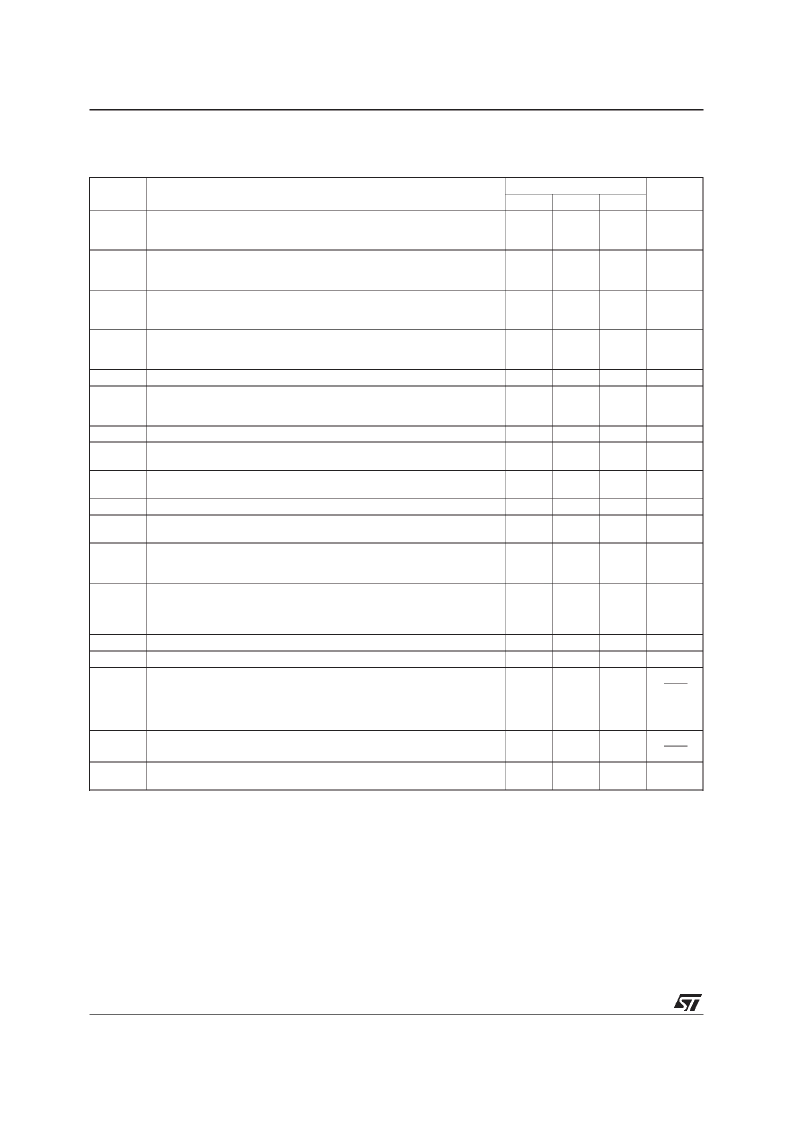
ELECTRICAL CHARACTERISTICS
LF355, LF356, LF357
0
o
C
≤
T
amb
≤
+70
o
C
V
CC
=
±
15V
, (unless otherwise specified)
Symbol
Parameter
LF355 - LF356 - LF357
Min.
Typ.
Unit
Max.
V
io
Input Offset Voltage (R
S
= 50
)
T
amb
= 25
o
C
T
min.
≤
T
amb
≤
T
max.
Input Offset Current - (note 3)
T
amb
= 25
o
C
T
min.
≤
T
amb
≤
T
max.
Input Bias Current - (note 3)
T
amb
= 25
C
T
min.
≤
T
amb
≤
T
max.
Large Signal Voltage Gain (R
L
= 2k
, V
O
=
±
10V)
T
amb
= 25
o
C
T
min.
≤
T
amb
≤
T
max.
Supply Voltage Rejection Ratio - (note 4)
Supply Current (no load)
T
amb
= 25
C
3
10
13
mV
I
io
3
50
2
pA
nA
I
ib
20
200
8
pA
nA
V/mV
A
vd
25
15
80
200
SVR
I
CC
100
dB
mA
LF355
LF356, LF357
2
5
5
4
10
DV
io
DV
io
/V
io
Input Offset Voltage Drift (R
S
= 50
) - (note 2)
Change in Average Temperature Coefficient with V
io
adjust
(R
S
= 50
)
Input Common Mode Voltage Range (T
amb
= 25
o
C)
μ
V/
o
C
μ
V/
o
C
per mV
V
0.5
V
icm
±
10
+15.1
-12
100
±
13
±
12
2.5
5
20
CMR
±
V
OPP
Common Mode Rejection Ratio
Output Voltage Swing
80
±
12
±
10
dB
V
R
L
= 10k
R
L
= 2k
LF355
LF356
LF357
GBP
Gain Bandwidth Product T
amb
= 25
o
C)
MHz
SR
Slew Rate (T
amb
= 25
o
C)
A
V
= 1
LF355
LF356
LF357
A
V
= 5
5
12
50
10
12
3
V/
μ
s
R
i
C
i
e
n
Input Resistance (T
amb
= 25
o
C)
Input Capacitance (Tamb = 25
o
C)
Equivalent Input Noise Voltage (T
amb
= 25
o
C, R
= 100
)
f = 1000Hz
pF
nV
√
Hz
LF355
LF356, LF357
LF355
LF356, LF357
f = 100Hz
20
12
25
15
i
n
Equivalent Input Noise Current
(T
amb
= 25
o
C, f = 100Hz or f = 1000Hz)
Settling Time (T
amb
= 25
o
C) - (note 5)
0.01
pA
√
Hz
μ
s
t
s
LF355
LF356, LF357
4
1.5
LF155 - LF156 - LF157
4/14
相關(guān)PDF資料 |
PDF描述 |
|---|---|
| LF356 | Wide Bandwidth Single J-FET Operational Amplifiers(寬帶J-FET單運放) |
| LF33CPT | VERY LOW DROP VOLTAGE REGULATORS WITH INHIBIT |
| LF33ABDT-TR | VERY LOW DROP VOLTAGE REGULATORS WITH INHIBIT |
| LF12ABV5V | GT 25C 25#16 SKT RECP WALL RM |
| LF15ABV5V | VERY LOW DROP VOLTAGE REGULATORS WITH INHIBIT |
相關(guān)代理商/技術(shù)參數(shù) |
參數(shù)描述 |
|---|---|
| LF257D | 制造商:STMICROELECTRONICS 制造商全稱:STMicroelectronics 功能描述:WIDE BANDWIDTH SINGLE J-FET OPERATIONAL AMPLIFIERS |
| LF257H | 制造商:NSC 制造商全稱:National Semiconductor 功能描述:Series Monolithic JFET Input Operational Amplifiers |
| LF257M | 制造商:未知廠家 制造商全稱:未知廠家 功能描述:Voltage-Feedback Operational Amplifier |
| LF257N | 制造商:STMICROELECTRONICS 制造商全稱:STMicroelectronics 功能描述:WIDE BANDWIDTH SINGLE J-FET OPERATIONAL AMPLIFIERS |
| LF25AB | 制造商:STMICROELECTRONICS 制造商全稱:STMicroelectronics 功能描述:Very low drop voltage regulators with inhibit |
發(fā)布緊急采購,3分鐘左右您將得到回復(fù)。