- 您現(xiàn)在的位置:買賣IC網(wǎng) > PDF目錄358772 > LC99012A-S (Sanyo Electric Co.,Ltd.) Black-and-White CCD Timing Generator PDF資料下載
參數(shù)資料
| 型號(hào): | LC99012A-S |
| 廠商: | Sanyo Electric Co.,Ltd. |
| 英文描述: | Black-and-White CCD Timing Generator |
| 中文描述: | 黑與白CCD時(shí)序發(fā)生器 |
| 文件頁(yè)數(shù): | 5/6頁(yè) |
| 文件大?。?/td> | 59K |
| 代理商: | LC99012A-S |
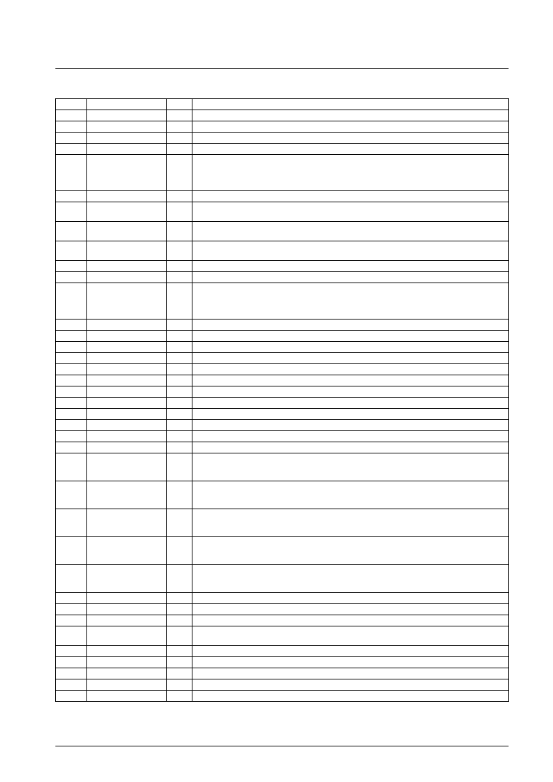
Pin Functions
Note:
*
Flickerless mode can be used when the auto-iris function is off, i.e. when EXT3 is high and EXT4 is low.
No. 5281-5/6
LC99012A-S
Pin No.
Symbol
I/O
Function
1
GND
2
PCO
O
Phase comparator output
3
AI
I
PCO output signal low-pass filter amplifier input
4
AO
O
PCO output signal low-pass filter amplifier output
Reference clock input (resonator inverter input)
LC9947G
:
28.63636 MHz
LC9948G: 28.375 MHz
LC9949G: 14.31818 MHz
5
CKI
I
6
CKO
O
Resonator inverter output
7
CCDSCAN
I
Low/open: CCD interlaced storage mode
High: CCD non-interlaced storage mode
8
SSGSCAN
I
Low/open: C.SYNC interlaced mode
High: C.SYNC non-interlaced mode
9
CLK14M
O
LC9947G/9949G: 14.31818 MHz
LC9948G: 14.1875 MHz
10
HD
O
HD output
11
VD
O
VD output
Field identifier signal
High: odd
Low: even
Must be tied high if SSGSCAN is high.
12
FLD
O
13
V
DD
KISYU
14
I
Must be tied high when used with the LC9949G. Otherwise must be tied low.
15
HR
I
Horizontal reset, C.SYNC reset, and vertical reset pulse input
16
VR
I
Vertical reset pulse input and external synchronization mode setup
17
GND
18
SELMET1
I
Light metering mode control
19
SELMET2
I
Light metering mode control
20
EXT1
I
External synchronization mode control
21
EXT2
I
External synchronization mode control
22
EXT3
I
CCD drive external control mode control
23
EXT4
I
CCD drive external control mode control
24
V
DD
I
Normally used to control the electronic iris step (rate of change)
Low: 1/8
Hifh: 1/16
25
STEPSTOP
I/O
Sensitivity increasing switch
Low/open: normal
High: Increased sensitivity mode
26
SENS
I
Increased sensitivity mode type switching
Low or open: In field units
High: In single scan line (1H) units
27
MSENS
I
Flickerless mode
*
switch
Low: Flickerless mode
High/open: normal
28
FLESS
I
CCD storage mode control
This pin must be left open or tied high when the LC99012A-S is used with an LC9947G/49G, and must
be tied low when used with an LC9948G.
29
STR
I
30
NSUB3
O
CCD NSUB pulses
31
NSUB2
O
CCD NSUB pulses
32
NSUB1
O
CCD NSUB pulses
33
TEST
I
Low: test mode
High/open: normal operating mode
34
VI1
O
CCD imaging block transfer clock (1)
35
VI3
O
CCD imaging block transfer clock (3)
36
VI2
O
CCD imaging block transfer clock (2)
37
VI4
O
CCD imaging block transfer clock (4)
38
VS4
O
CCD imaging block transfer clock (S4)
Continued on next page.
相關(guān)PDF資料 |
PDF描述 |
|---|---|
| LC99052-V64A | Image Sensor Control LSI |
| LC99053 | SMD LED Lamps |
| LC99062-W50 | Image Sensor Signal Processing LSI(圖象傳感信號(hào)處理LSI) |
| LC99063-LF2 | CCD Digital Signal Processing IC(CCD(電耦合器件)數(shù)字信號(hào)處理芯片) |
| LC9907 | Timing Generator for Solid-State Imager |
相關(guān)代理商/技術(shù)參數(shù) |
參數(shù)描述 |
|---|---|
| LC99052-V64A | 制造商:SANYO 制造商全稱:Sanyo Semicon Device 功能描述:Image Sensor Control LSI |
| LC99053 | 制造商:SANYO 制造商全稱:Sanyo Semicon Device 功能描述:CMOS LSI |
| LC99057-LA8 | 制造商:未知廠家 制造商全稱:未知廠家 功能描述:Signal Conditioner |
| LC99059-MJ9 | 制造商:未知廠家 制造商全稱:未知廠家 功能描述:Signal Conditioner |
| LC99062-W50 | 制造商:SANYO 制造商全稱:Sanyo Semicon Device 功能描述:Image Sensor Signal Processing LSI |
發(fā)布緊急采購(gòu),3分鐘左右您將得到回復(fù)。