- 您現(xiàn)在的位置:買賣IC網(wǎng) > PDF目錄358768 > LC863516B (Sanyo Electric Co.,Ltd.) 8-bit 1-chip Microcontroller PDF資料下載
參數(shù)資料
| 型號: | LC863516B |
| 廠商: | Sanyo Electric Co.,Ltd. |
| 英文描述: | 8-bit 1-chip Microcontroller |
| 中文描述: | 8位1片上微控制器 |
| 文件頁數(shù): | 8/17頁 |
| 文件大?。?/td> | 527K |
| 代理商: | LC863516B |
LC863548B/40B/32B/28B/24B/20B/16B
No.7936-8/17
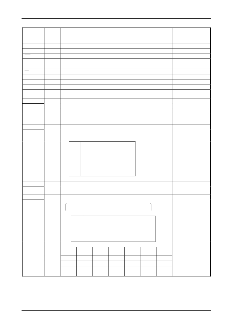
Pin Description
Pin name
I/O
Function
Option
VSS
XT1
-
Negative power supply
I
Input terminal for crystal oscillator
XT2
O
Output terminal for crystal oscillator
VDD
RES
-
Positive power supply
I
Reset terminal
FILT
O
Filter terminal for PLL
VS
I
Vertical synchronization signal input terminal
HS
I
Horizontal synchronization signal input terminal
R
O
Red (R) output terminal of RGB image output
G
O
Green (G) output terminal of RGB image output
B
O
Blue (B) output terminal of RGB image output
BL
O
Fast blanking control signal
Switch TV image signal and caption/OSD image signal
Port 0
P00 to P07
I/O
8-bit input/output port
Input/output can be specified in nibble unit
(If the N-ch open drain output is selected by option, the corresponding port data can be
read in output mode.)
Other functions
AD converter input port (P04 to P07 : 4 channels)
Pull-up resistor
provided/not provided
Output Format
CMOS/Nch-OD
Port 1
8-bit input/output port
Input/output can be specified for each bit
(programmable pull-up resister provided)
Other functions
P10
P11
P12
P13
P14
P15
P16
P17
IIC0 data I/O
IIC0 clock output
IIC1 data I/O
IIC1 clock output
PWM1 output
PWM2 output
PWM3 output
Timer 1 (PWM) output
P10 to P17
I/O
Output Format
CMOS/Nch-OD
Port 3
P30 to P33
I/O
4-bit input/output port
Input/output can be specified for each bit
(CMOS output/input with programmable pull-up resister)
Port 7
4-bit input/output port
Input or output can be specified for each bit
P70 : I/O with programmable pull-up resister
P71 to P73 : CMOS output/input with programmable pull-up resister
Other function
P70
P71
P72
P73
INT0 input/HOLD release input/
Nch-Tr. Output for watchdog timer
INT1 input/HOLD release input
INT2 input/Timer 0 event input
INT3 input (noise rejection filter connected) /
Timer 0 event input
Interrupt receiver format, vector addresses
rising
falling
rising/
falling
H level
L level
vector
INT0
enable
enable
disable
enable
enable
03H
INT1
enable
enable
disable
enable
enable
0BH
INT2
enable
enable
enable
disable
disable
13H
P70
P71 to P73
I/O
INT3
enable
enable
enable
disable
disable
1BH
Note : A capacitor of at least 10
μ
F must be inserted between VDD and VSS when using this IC.
Continued on next page.
相關PDF資料 |
PDF描述 |
|---|---|
| LC863516 | LC86F3548A |
| LC864112B | 8-bit Microcontroller with 2/4/8K Bytes In-System Programmable Flash |
| LC864112 | 8-Bit Single Chip Microcontroller |
| LC864140B | 8-Bit Single Chip Microcontroller |
| LC864265A | 8-bit Microcontroller with 2/4/8K Bytes In-System Programmable Flash |
相關代理商/技術參數(shù) |
參數(shù)描述 |
|---|---|
| LC863516C | 制造商:SANYO 制造商全稱:Sanyo Semicon Device 功能描述:8-bit 1-chip Microcontroller |
| LC863520 | 制造商:SANYO 制造商全稱:Sanyo Semicon Device 功能描述:LC86F3548A |
| LC863520A | 制造商:SANYO 制造商全稱:Sanyo Semicon Device 功能描述:8-Bit Single-Chip Microcontroller |
| LC863520B | 制造商:SANYO 制造商全稱:Sanyo Semicon Device 功能描述:8-bit 1-chip Microcontroller |
| LC863524 | 制造商:SANYO 制造商全稱:Sanyo Semicon Device 功能描述:8-Bit Single-Chip Microcontroller |
發(fā)布緊急采購,3分鐘左右您將得到回復。