- 您現(xiàn)在的位置:買賣IC網(wǎng) > PDF目錄358767 > LC7942KD (Sanyo Electric Co.,Ltd.) CMOS IC Dot-Matrix LCD Drivers PDF資料下載
參數(shù)資料
| 型號: | LC7942KD |
| 廠商: | Sanyo Electric Co.,Ltd. |
| 英文描述: | CMOS IC Dot-Matrix LCD Drivers |
| 中文描述: | CMOS集成電路點陣LCD驅(qū)動器 |
| 文件頁數(shù): | 5/8頁 |
| 文件大小: | 76K |
| 代理商: | LC7942KD |
LC7942KD
No.A0575-5/8
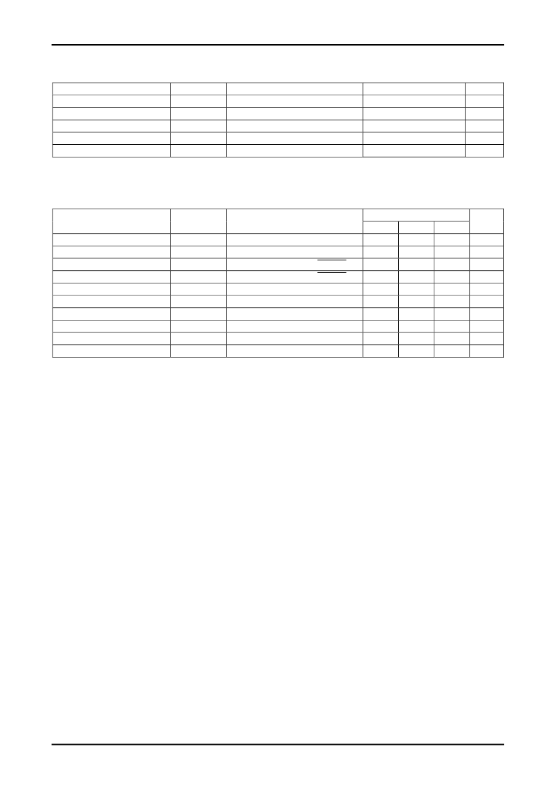
Specifications
Absolute Maximum Ratings
at Ta=25
±
2
°
C, VSS = 0V
Parameter
Symbol
Conditions
Ratings
Unit
Maximum supply voltage (logic)
VDD max
VDD-VEE max
VIN max
Topr
-
-0.3 to +7.0
V
Maximum supply voltage (LCD)
*1
0 to 22
V
Maximum input voltage
-
-0.3 to VDD +0.3
-20 to +85
V
Operating temperature range
-
°
C
Storage temperature range
Note
*
1 The voltages V1, V2, and V5 must obey the relationships:
VDD
≥
V1>V2>V5>VEE, VDD-V2
≤
7V, V5-VEE
≤
7V
Allowable Operating Ranges
at Ta = -20 to 85
°
C, VSS = 0V
Tstg
-
-40 to +125
°
C
Ratings
Parameter
Symbol
Conditions
min
typ
max
Unit
Supply voltage (logic)
VDD
VDD-VEE
VIH
VIL
fCP
tWC
tSETUP
tHOLD
tR
tF
-
2.7
-
5.5
V
Supply voltage (LCD)
*2, 3
8
-
20
V
Input high level voltage
DIO1, DIO64, CP, M, RS/LS, DISPOFF
0.8VDD
-
-
-
V
Input low level voltage
DIO1, DIO64, CP, M, RS/LS, DISPOFF
-
0.2VDD
V
CP (Shift clock)
CP
-
-
1
MHz
CP (pulse width)
CP
125
-
-
ns
Setup time
DIO1
→
CP, DIO64
→
CP
100
-
-
ns
Hold time
DIO1
→
CP, DIO64
→
CP
100
-
-
ns
CP rise time
CP
-
-
50
ns
CP fall time
Note
*
2 The voltages V1, V2, and V5 must obey the relationships:
VDD
≥
V1>V2>V5>VEE, VDD-V2
≤
7V, V5-VEE
≤
7V
*
3 When applying power, apply power to the LCD drive block after applying power to the logic block or apply
power to both the blocks simultaneously. When turning off power, turn off power to the logic block after
turning off power to the LCD drive block or turn off power to both the blocks simultaneously.
CP
-
-
50
ns
相關(guān)PDF資料 |
PDF描述 |
|---|---|
| LC7942ND | Dot Matrix LCD Driver(點陣LCD驅(qū)動器) |
| LC7942YC | Dot Matrix LCD Driver(點陣LCD驅(qū)動器) |
| LC7942YD | Dot Matrix LCD Driver(點陣LCD驅(qū)動器) |
| LC79430 | Dot Matrix LCD Driver |
| LC79430D | Dot Matrix LCD Driver |
相關(guān)代理商/技術(shù)參數(shù) |
參數(shù)描述 |
|---|---|
| LC7942ND | 制造商:SANYO 制造商全稱:Sanyo Semicon Device 功能描述:Dot-Matrix LCD Driver |
| LC7942ND-E | 制造商:SANYO Semiconductor Co Ltd 功能描述: |
| LC7942YC | 制造商:未知廠家 制造商全稱:未知廠家 功能描述:Interface IC |
| LC7942YD | 制造商:未知廠家 制造商全稱:未知廠家 功能描述: |
| LC7943 | 制造商:未知廠家 制造商全稱:未知廠家 功能描述:Interface IC |
發(fā)布緊急采購,3分鐘左右您將得到回復。