- 您現(xiàn)在的位置:買賣IC網(wǎng) > PDF目錄358764 > LC75741 (Sanyo Electric Co.,Ltd.) 1/2 Duty Driver for Frequency Displays PDF資料下載
參數(shù)資料
| 型號: | LC75741 |
| 廠商: | Sanyo Electric Co.,Ltd. |
| 英文描述: | 1/2 Duty Driver for Frequency Displays |
| 中文描述: | 1 / 2的責(zé)任驅(qū)動頻率顯示 |
| 文件頁數(shù): | 9/18頁 |
| 文件大?。?/td> | 308K |
| 代理商: | LC75741 |

Output Data
KD1 to KD30: Key data
These bits represent the key output states when a key matrix with up to 30 keys is formed using the KS1 to KS6 key
scan output pins and the KI1 to KI5 key scan input pins. When a key is pressed, the bit corresponding to that key will
be set to 1. The correspondence is listed in the following table.
SA: Sleep acknowledge data
This output data is set to the state when the key was pressed. In that case DO will go to the low level. If serial data is
input during this period and the mode is set (normal mode or sleep mode), the IC will be set to that mode. SA is set to
1 in the sleep mode and to 0 in the normal mode.
Sleep Mode
The IC is set to sleep mode by setting either S0 or S1 in the control data to 1. The segment outputs and the digit outputs
are all set low, and the clock generator (oscillator circuit) is stopped (although it is restarted when a key is pressed), and
thus power dissipation is reduced. This mode is cleared by setting S0 and S1 in the control data to 0.
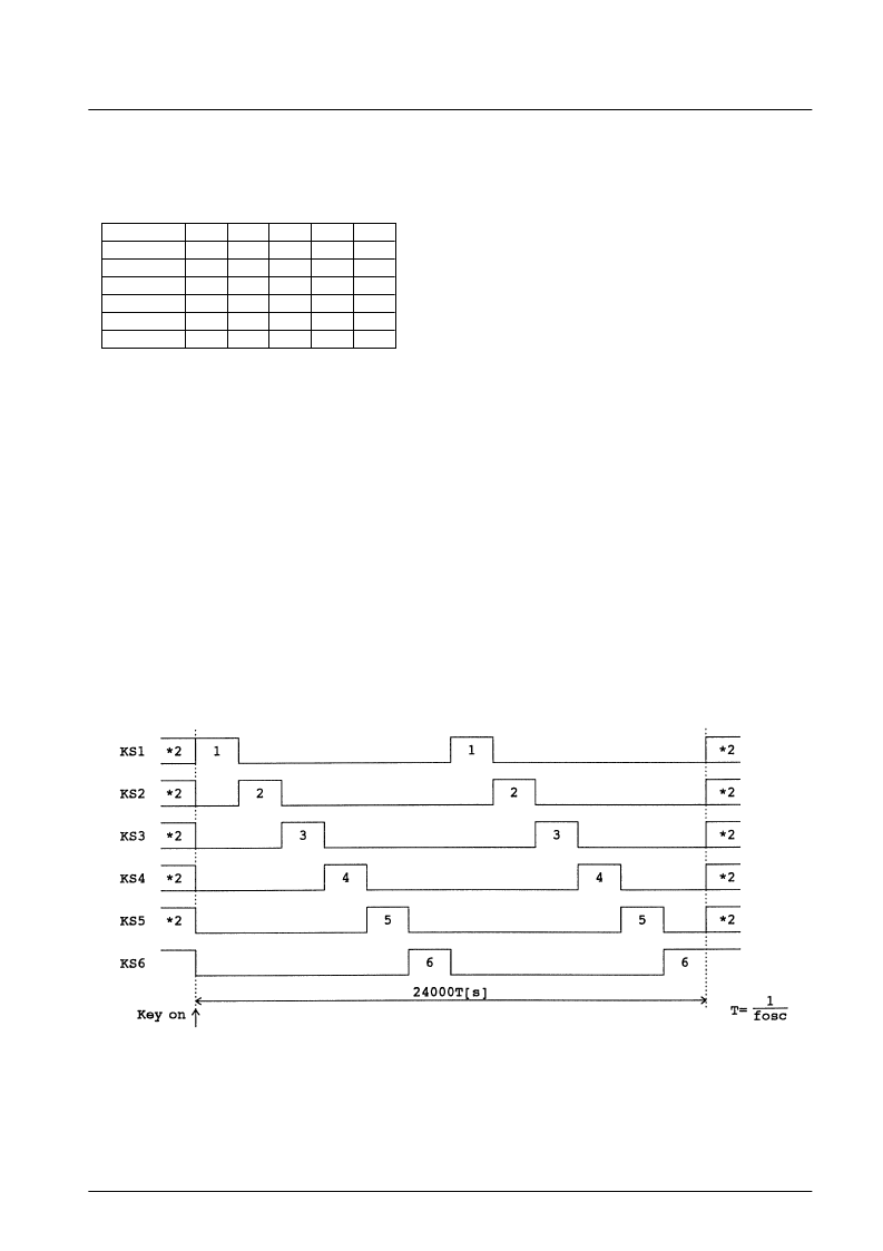
Key Scan Operation
Key scan timing
The scan period is 12000T [s]. A key scan is performed twice to reliably recognize the key on/off states by verifying
that the key data for the two scans agrees. If the data agrees, the IC recognizes a key press and 25600T [s] after the
start of key scan execution issues a key scan data read request by outputting a low level from DO. If the key data does
not agree and a key was pressed at the later scan, the IC executes another key scan operation. Note that this means that
this IC cannot recognize a key press shorter than 25600T [s].
Note
*
: The high-level and low-level states in sleep mode are set according to the control data S0 and S1. Key scan output signals are not output from pins
set to the “L” state.
No. 6142-9/18
LC75742E, LC75742W
Item
KI1
KI2
KI3
KI4
KI5
KS1
KD1
KD2
KD3
KD4
KD5
KS2
KD6
KD7
KD8
KD9
KD10
KS3
KD11
KD12
KD13
KD14
KD15
KS4
KD16
KD17
KD18
KD19
KD20
KS5
KD21
KD22
KD23
KD24
KD25
KS6
KD26
KD27
KD28
KD29
KD30
相關(guān)PDF資料 |
PDF描述 |
|---|---|
| LC75741E | 1/2 Duty Driver for Frequency Displays |
| LC75742E | RES 36K OHM 1/8W 5% 0805 SMD |
| LC75742W | 1/2 Duty VFD Driver with Key Input Function |
| LC75750W | 1/3 Duty VFD Driver(1/3占空VFD顯示驅(qū)動器) |
| LC75754M | 1/3 Duty VFD Driver(1/3占空VFD顯示驅(qū)動器) |
相關(guān)代理商/技術(shù)參數(shù) |
參數(shù)描述 |
|---|---|
| LC75741E | 制造商:SANYO 制造商全稱:Sanyo Semicon Device 功能描述:1/2 Duty Driver for Frequency Displays |
| LC75741W | 制造商:SANYO 制造商全稱:Sanyo Semicon Device 功能描述:1/2 Duty Driver for Frequency Displays |
| LC75742E | 制造商:SANYO 制造商全稱:Sanyo Semicon Device 功能描述:1/2 Duty VFD Driver with Key Input Function |
| LC75742W | 制造商:SANYO 制造商全稱:Sanyo Semicon Device 功能描述:1/2 Duty VFD Driver with Key Input Function |
| LC7574E | 制造商:未知廠家 制造商全稱:未知廠家 功能描述:Vacuum Fluorescent Display Driver |
發(fā)布緊急采購,3分鐘左右您將得到回復(fù)。