- 您現(xiàn)在的位置:買賣IC網(wǎng) > PDF目錄358761 > LC73861 (Sanyo Electric Co.,Ltd.) DTMF Receiver LSI PDF資料下載
參數(shù)資料
| 型號: | LC73861 |
| 廠商: | Sanyo Electric Co.,Ltd. |
| 英文描述: | DTMF Receiver LSI |
| 中文描述: | 雙音多頻接收器大規(guī)模集成電路 |
| 文件頁數(shù): | 2/5頁 |
| 文件大小: | 73K |
| 代理商: | LC73861 |
AC Electrical Characteristics
at Ta = 25°C
±
2°C, V
DD
= 5 V, V
SS
= 0 V, f
OSC
= 4.194304 MHz
Parameter
Symbol
Conditions
min
–49.5
typ
max
Unit
dBm
dB
Hz
%
dB
dB
dB
ms
ms
MHz
ns
ns
ns
MHz
MHz
pF
Valid input signal level
Positive twist accept
Frequency deviation accept
Frequency deviation reject
Third tone tolerance
Dial tone tolerance
Noise tolerance
Tone present detect time
Tone absent detect time
Data shift rate
Data output delay time
Setup time delay
Data hold time
See notes 1, 2, 3, 5, 6 and 9.
See notes 2, 3, 4, 9 and 11.
See notes 2, 3, 5 and 9.
See notes 2, 3 and 5.
See notes 2, 3, 4, 5, 9 and 10.
See notes 2, 3, 4, 5, 8, 9 and 10.
See notes 2, 3, 4, 5, 7, 9 and 10.
See Timing Chart.
See Timing Chart.
0
6
±
1.5%
±
2
±
3.5
–16
22
–12
t
DP
t
DA
3
20
20
1
0.5
t
PAD
t
DL
t
DH
See Timing Chart.
See Timing Chart.
See Timing Chart.
LC73861
LC73862
OSCI and OSCO
100
0
30
Oscillator frequency
f
OSC
4.190109 4.194304 4.198498
3.5759
3.5795
3.5831
Load capacitance
C
XO
30
Notes
1.
2.
3.
4.
5.
6.
7.
8.
9.
10. Referenced to the lowest frequency component of the DTMF signal.
11. Twist = High-frequency group tone level
÷
Low-frequency group tone level.
0 dBm = 1 mW power when driving a 600
load.
All 16 DTMF signal frequencies.
40 ms DTMF signal period and 40 ms pause period.
Nominal DTMF frequency.
Low-frequency group and High-frequency group signal levels are the same.
DTMF signal frequency deviation is within
±
1.5%
±
2 Hz.
Bandwidth limited (0 to 3 kHz) Gaussian noise.
350 Hz and 440 Hz dial tone frequencies.
Error rate of less than 1 in 10,000.
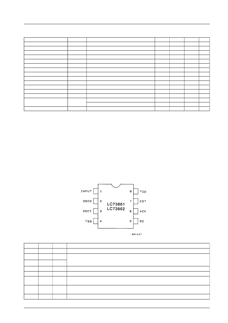
Pin Assignment
Pin Description
Number
1
2
Name
INPUT
OSCO
I/O
I
O
Description
Input coupling capacitor required. Biased internally to V
DD
/2.
An oscillating circuit is formed by connecting a 4.194304 MHz (LC73861) / 3.579545 MHz (LC73826)
oscillator and a capacitor (if needed) between these pins. (To determine whether an external
capacitor is needed or not, contact the manufacturer of the oscillator.)
Supply pin, normally 0 V
Outputs 4-bit serial decoded DTMF output, least significant bit first.
The ACK pin is used to shift out data to the SD pin. Four pulses are needed in order to shift out the
4-bit DTMF code. The data is latched by the shift register before the rising edge of the first pulse.
Indicates the presence of a DTMF signal when HIGH. (This pin can be monitored and after a short
delay, data can be accessed by 4 pulses to ACK.)
Supply pin, normally 4.5 V to 5.5 V
3
OSCI
I
4
5
6
V
SS
SD
ACK
O
I
7
EST
O
8
V
DD
O
Top view
LC73861, LC73862
No.4431-2/5
相關(guān)PDF資料 |
PDF描述 |
|---|---|
| LC73872 | DTMF Receiver |
| LC73872M | DTMF Receiver |
| LC7387M | DTMF Receiver |
| LC73881M | DTMF Receiver LSI |
| LC7410 | CMOS LSI VTR(B/VHS) SERVO CIRCUIT |
相關(guān)代理商/技術(shù)參數(shù) |
參數(shù)描述 |
|---|---|
| LC73862 | 制造商:SANYO 制造商全稱:Sanyo Semicon Device 功能描述:DTMF Receiver LSI |
| LC73872 | 制造商:SANYO 制造商全稱:Sanyo Semicon Device 功能描述:DTMF Receiver |
| LC73872M | 制造商:SANYO 制造商全稱:Sanyo Semicon Device 功能描述:DTMF Receiver |
| LC73872MK-TRM-E | 制造商:ON Semiconductor 功能描述:DATA COMMUNICATION ICS - Tape and Reel |
| LC73872M-TRM-E | 制造商:ON Semiconductor 功能描述:DATA COMMUNICATION ICS - Tape and Reel |
發(fā)布緊急采購,3分鐘左右您將得到回復(fù)。