- 您現(xiàn)在的位置:買賣IC網(wǎng) > PDF目錄358760 > LC72725KM (Sanyo Electric Co.,Ltd.) CMOS IC RDS(RBDS) Demodulation IC PDF資料下載
參數(shù)資料
| 型號: | LC72725KM |
| 廠商: | Sanyo Electric Co.,Ltd. |
| 英文描述: | CMOS IC RDS(RBDS) Demodulation IC |
| 中文描述: | CMOS集成電路的RDS(RBDS)的解調(diào)芯片 |
| 文件頁數(shù): | 9/9頁 |
| 文件大小: | 181K |
| 代理商: | LC72725KM |
LC72725KM, 72725KV
No.A0503-9/9
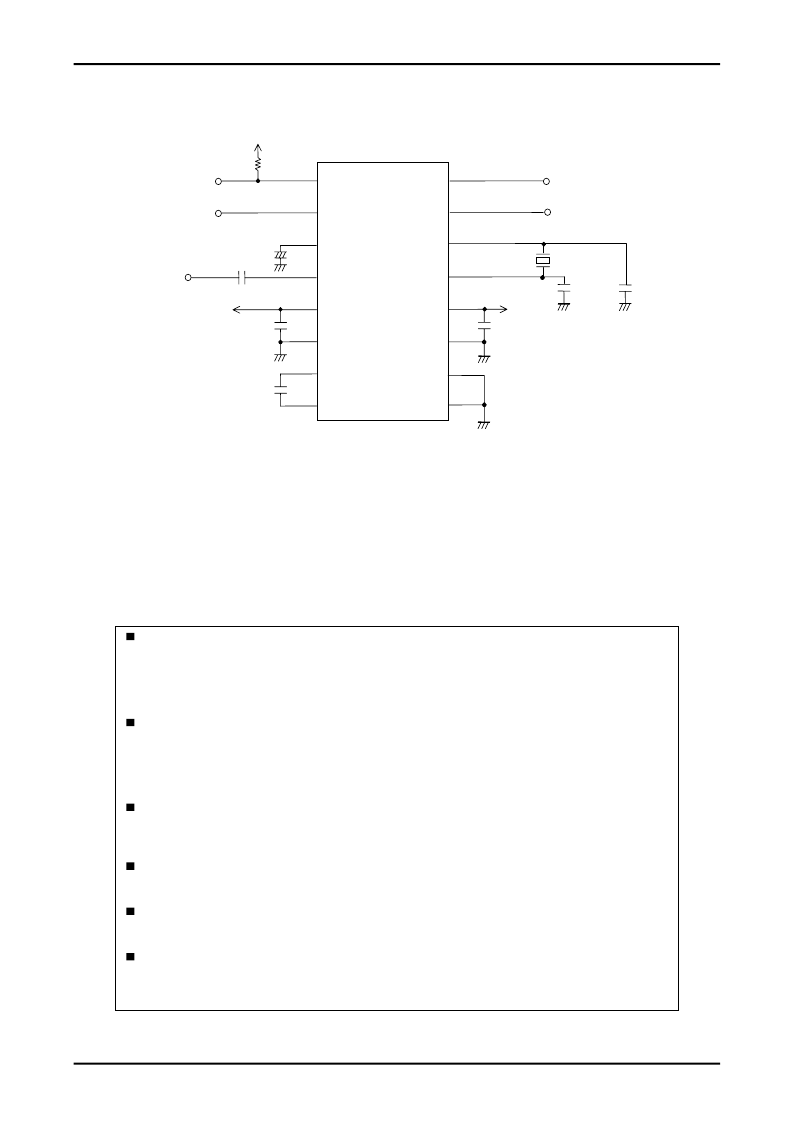
Sample Application Connection Circuit (for master mode operation)
Note: If the RST pin is unused, it must be connected to ground.
PS
This catalog provides information as of September, 2006. Specifications and information herein are subject
to change without notice.
Specifications of any and all SANYO Semiconductor products described or contained herein stipulate the
performance, characteristics, and functions of the described products in the independent state, and are
not guarantees of the performance, characteristics, and functions of the described products as mounted
in the customer's products or equipment. To verify symptoms and states that cannot be evaluated in an
independent device, the customer should always evaluate and test devices mounted in the customer's
products or equipment.
SANYO Semiconductor Co., Ltd. strives to supply high-quality high-reliability products. However, any
and all semiconductor products fail with some probability. It is possible that these probabilistic failures
could give rise to accidents or events that could endanger human lives, that could give rise to smoke or
fire, or that could cause damage to other property. When designing equipment, adopt safety measures
so that these kinds of accidents or events cannot occur. Such measures include but are not limited to
protective circuits and error prevention circuits for safe design, redundant design, and structural design.
In the event that any or all SANYO Semiconductor products (including technical data,services) described
or contained herein are controlled under any of applicable local export control laws and regulations, such
products must not be exported without obtaining the export license from the authorities concerned in
accordance with the above law.
No part of this publication may be reproduced or transmitted in any form or by any means, electronic or
mechanical, including photocopying and recording, or any information storage or retrieval system, or
otherwise, without the prior written permission of SANYO Semiconductor Co., Ltd.
Any and all information described or contained herein are subject to change without notice due to
product/technology improvement, etc. When designing equipment, refer to the "Delivery Specification"
for the SANYO Semiconductor product that you intend to use.
Information (including circuit diagrams and circuit parameters) herein is for example only; it is not
guaranteed for volume production. SANYO Semiconductor believes information herein is accurate and
reliable, but no guarantees are made or implied regarding its use or any infringements of intellectual
property rights or other rights of third parties.
XOUT
TEST
VSSd
1
2
16
15
14
RDCL
RST
13
9
XIN
MODE
RST
RDCL
RDSID/READY
4.332MHz
VSSd
22pF
VSSd
22pF
CIN
FLOUT
VSSa
VSSa
VDDa
VDDa
8
7
6
5
4
+
3
10
μ
F
VSSa
MPXIN
MPXIN
560pF
0.1
μ
F
330pF
VREF
VSSd
VDDd
12
11
VSSd
0.1
μ
F
VDDd
VDDd
10k
RDSID/READY
RDDA
RDDA
10
相關(guān)PDF資料 |
PDF描述 |
|---|---|
| LC72725M | CMOS LSI |
| LC72725NV | RES FIX, .25W 1% 13.3K MET FLM |
| LC72725V | CMOS LSI |
| LC72E32 | Single-Chip Microcontroller Plus PLL LSI with On-Chip UVEPROM |
| LC72F3661 | CMOS IC Electronic tuning radio for car audio ETR Controller |
相關(guān)代理商/技術(shù)參數(shù) |
參數(shù)描述 |
|---|---|
| LC72725KM_10 | 制造商:SANYO 制造商全稱:Sanyo Semicon Device 功能描述:RDS(RBDS) Demodulation IC |
| LC72725KMA | 制造商:SANYO 制造商全稱:Sanyo Semicon Device 功能描述:RDS(RBDS) Demodulation IC |
| LC72725KMA-AH | 制造商:ON Semiconductor 功能描述:RDS DEMODULATION IC - Tape and Reel 制造商:ON Semiconductor 功能描述:REEL / RDS DEMODULATION IC |
| LC72725KMA-ZH | 功能描述:調(diào)節(jié)器/解調(diào)器 RoHS:否 制造商:Texas Instruments 封裝 / 箱體:PVQFN-N24 封裝:Reel |
| LC72725KM-TLM-E | 功能描述:音頻 DSP RDS DEMODULATION IC RoHS:否 制造商:Texas Instruments 工作電源電壓: 電源電流: 工作溫度范圍: 安裝風(fēng)格: 封裝 / 箱體: 封裝:Tube |
發(fā)布緊急采購,3分鐘左右您將得到回復(fù)。