- 您現(xiàn)在的位置:買賣IC網(wǎng) > PDF目錄358759 > LC72341G (Sanyo Electric Co.,Ltd.) Low-Voltage Single-Chip Microcontrollers with On-Chip PLL and LCD Driver Circuits(用于音頻設(shè)備的低電壓?jiǎn)纹⒖刂破鳎◣湘i相環(huán)電路和LCD驅(qū)動(dòng)器)) PDF資料下載
參數(shù)資料
| 型號(hào): | LC72341G |
| 廠商: | Sanyo Electric Co.,Ltd. |
| 英文描述: | Low-Voltage Single-Chip Microcontrollers with On-Chip PLL and LCD Driver Circuits(用于音頻設(shè)備的低電壓?jiǎn)纹⒖刂破鳎◣湘i相環(huán)電路和LCD驅(qū)動(dòng)器)) |
| 中文描述: | 低電壓的單芯片微控制器芯片PLL和LCD驅(qū)動(dòng)電路(用于音頻設(shè)備的低電壓?jiǎn)纹⒖刂破鳎◣湘i相環(huán)電路和液晶顯示驅(qū)動(dòng)器)) |
| 文件頁數(shù): | 8/12頁 |
| 文件大小: | 171K |
| 代理商: | LC72341G |

No. 5799-8/12
LC72341G/W, 72342G/W, 72343G/W
Continued from preceding page.
Pin No.
Pin
I/O
Function
I/O circuit
25
26
27
28
29
30
31
32
PG3/S20
PG2/S19
PG1/S18
PG0/S17
PH3/S16
PH2/S15
PH1/S14
PH0/S13
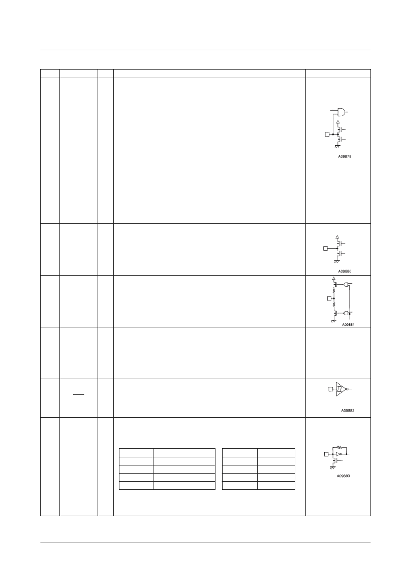
I/O
LCD driver segment output and general-purpose I/O shared function ports. The IOS
instruction is used for switching both between the segment output and general-purpose
I/O functions and between input and output for the general-purpose I/O port function.
*
When used as segment output ports
The general-purpose I/O port function is selected with the IOS instruction (Pwn = 8).
b0 = S17 to 20/PG0 to 3 (0: Segment output, 1: PG0 to 3)
The general-purpose I/O port function is selected with the IOS instruction (Pwn = 9).
b0 = S13 to 16/PH0 to 3 (0: Segment output, 1: PH0 to 3)
When used as general-purpose I/O ports
The IOS instruction (Pwn = 6,7) is used to select input or output. Note that the mode can
be set in a bit unit.
b0 = PG0
b1 = PG1 [0: Input, 1: Output]
b2 = PG2
b3 = PG3
In backup mode, these pins go to the input disabled, high-impedance state if set up as
general-purpose outputs, and are fixed at the low level if set up as segment outputs.
These ports are set up as segment outputs after a reset.
Although the general-purpose port/LCD port setting is a mask option, the IOS instruction
must be used as described above to set up the port function.
b0 = PH0
b1 = PH1 [0: Input, 1: Output]
b2 = PH2
b3 = PH3
CMOS push-pull circuit
S16 to
S1
33 to 44
O
LCD driver segment output pins.
A 1/4-duty 1/2-bias drive technique is used.
The frame frequency is 75 Hz.
In backup mode, the outputs are fixed at the low level.
After a reset, the outputs are fixed at the low level.
CMOS push-pull circuit
COM4
COM3
COM2
COM1
45
46
47
48
O
LCD driver common output pins.
A 1/4-duty 1/2-bias drive technique is used.
The frame frequency is 75 Hz.
In backup mode, the outputs are fixed at the low level.
After a reset, the outputs are fixed at the low level.
DBR4
DBR3
DBR2
DBR1
49
50
51
52
—
LCD power supply stepped-up voltage pins.
53
RES
I
System reset input.
In CPU operating mode or halt mode, applications must apply a low level for at least one
full machine cycle to reset the system and restart execution with the PC set to location 0.
This pin is connected in parallel with the internal power on reset circuit.
70
HCTR
I
Universal counter dedicated input port.
When taking frequency measurements, select the HCTR frequency measurement mode
and measurement time with the UCS instruction (b3 = 0, b2 = 0) and start the count with
a UCCinstruction.
The CNTEND flag is set when the count completes. Since this circuit functions as an AC
amplifier, always use capacitor coupling with the input signal. Input is disabled in backup
mode, in halt mode, after a reset, and in PLL stop mode.
UCS
b3,
b2
Input pin
Measurement mode
0
0
HCTR
Frequency measurement
0
1
—
1
0
—
1
1
—
UCS
b1,
b0
Measurement time
0
0
1 ms
0
1
4 ms
1
0
8 ms
1
1
32 ms
Continued on next page.
CMOS amplifier input
Note:
*
Applications must establish the output data in advance with an OUT, SPB, or RPB instruction and then set the pin to output mode with an IOS
instruction when using the I/O switchable ports as output pins.
相關(guān)PDF資料 |
PDF描述 |
|---|---|
| LC72345 | Low-Voltage ETR Controller with On-Chip DC-DC Converter |
| LC72346 | Ultralow-Voltage ETR Controller with On-Chip LCD Driver |
| LC72346W | Ultralow-Voltage ETR Controller with On-Chip LCD Driver |
| LC72349 | Low-Voltage ETR Controller with On-Chip LCD Driver |
| LC72349W | Low-Voltage ETR Controller with On-Chip LCD Driver |
相關(guān)代理商/技術(shù)參數(shù) |
參數(shù)描述 |
|---|---|
| LC72341W | 制造商:SANYO 制造商全稱:Sanyo Semicon Device 功能描述:Low-Voltage Single-Chip Microcontrollers with On- Chip PLL and LCD Driver Circuits |
| LC72342G | 制造商:SANYO 制造商全稱:Sanyo Semicon Device 功能描述:Low-Voltage Single-Chip Microcontrollers with On- Chip PLL and LCD Driver Circuits |
| LC72342W | 制造商:SANYO 制造商全稱:Sanyo Semicon Device 功能描述:Low-Voltage Single-Chip Microcontrollers with On- Chip PLL and LCD Driver Circuits |
| LC72342-XXXX | 制造商:未知廠家 制造商全稱:未知廠家 功能描述: |
| LC72343G | 制造商:SANYO 制造商全稱:Sanyo Semicon Device 功能描述:Low-Voltage Single-Chip Microcontrollers with On- Chip PLL and LCD Driver Circuits |
發(fā)布緊急采購(gòu),3分鐘左右您將得到回復(fù)。