- 您現(xiàn)在的位置:買賣IC網(wǎng) > PDF目錄30730 > LC7074 SPECIALTY CONSUMER CIRCUIT, PDIP18 PDF資料下載
參數(shù)資料
| 型號: | LC7074 |
| 元件分類: | 消費家電 |
| 英文描述: | SPECIALTY CONSUMER CIRCUIT, PDIP18 |
| 封裝: | DIP-18 |
| 文件頁數(shù): | 3/17頁 |
| 文件大?。?/td> | 237K |
| 代理商: | LC7074 |

LC7074, 7074M
No.4789–11/17
4. Informative Bits in the Serial Data Output
Error Flag (E) and Correction Flag (F)
The error flag (E) and the correction flag (F) in the serial data output are identical to the ERROR and CORRECTION
output pins, except that the logical levels are inverted.
The meaning of the error and correction flags differ slightly depending on the setting that determines whether input
data error correction is to be performed (the CORR.SEL pin). The tables below show the relations between the output
value combinations of the error and correction flags.
– When the CORR.SEL pin is high: Error correction enabled
The value combination where E is 1 and F is 0 (or equivalently, where the ERROR pin is 0 and the CORRECTION
pin is 1) cannot occur.
– When the CORR.SEL pin is high: Error correction disabled
The value combination where E is 1 and F is 0 (or equivalently, where the ERROR pin is 0 and the CORRECTION
pin is 1) and where E is 0 and F is 1 (or equivalently, where the ERROR pin is 1 and the CORRECTION pin is 0)
cannot occur.
In this case, the combination indicating no errors is output if there were no errors in the data, and the combination
indicating uncorrectable errors is output when there are errors in the data whether or not those errors are correctable.
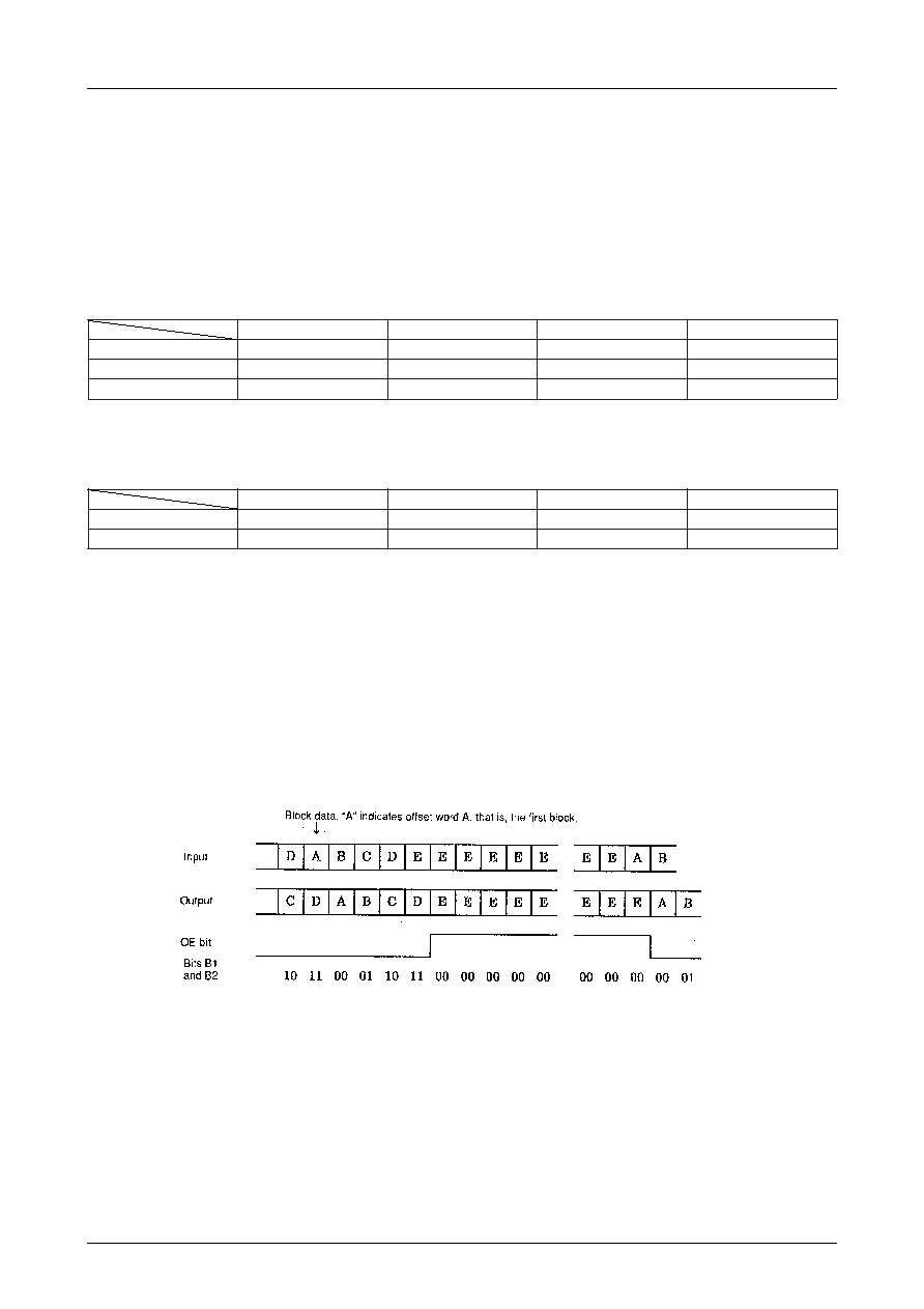
Offset E (OE) and Offset F (OF)
When the IC has synchronized with the offset word E block data, the OE bit in the output data goes to “1”. At this
point the bits B1 and B0, which express the RDS block number, will be “00”, i.e., both will be zero.
The LC7074/M does not recognize an offset word F block as a correct offset word. Therefore, the OF bit in the output
data will always be “0”.
OE Bit Output
)
E
(
g
a
l
f
r
o
r
E)
F
(
g
a
l
f
n
o
i
t
c
e
r
o
Cn
i
p
R
O
R
En
i
p
N
O
I
T
C
E
R
O
C
s
r
o
r
e
o
N
0011
d
e
t
c
e
r
o
c
s
r
o
r
E
0110
s
r
o
r
e
l
b
a
t
c
e
r
o
c
n
U
1100
)
E
(
g
a
l
f
r
o
r
E)
F
(
g
a
l
f
n
o
i
t
c
e
r
o
Cn
i
p
R
O
R
En
i
p
N
O
I
T
C
E
R
O
C
s
r
o
r
e
o
N
0011
s
r
o
r
e
l
b
a
t
c
e
r
o
c
n
U
1100
相關(guān)PDF資料 |
PDF描述 |
|---|---|
| LC7074M | SPECIALTY CONSUMER CIRCUIT, PDSO18 |
| LC7152KM | PLL FREQUENCY SYNTHESIZER, 80 MHz, PDSO24 |
| LC7152NM | PLL FREQUENCY SYNTHESIZER, 55 MHz, PDSO24 |
| LC7152 | PLL FREQUENCY SYNTHESIZER, 55 MHz, PDIP24 |
| LC72131KM | PLL FREQUENCY SYNTHESIZER, 40 MHz, PDSO20 |
相關(guān)代理商/技術(shù)參數(shù) |
參數(shù)描述 |
|---|---|
| LC7074M | 制造商:SANYO 制造商全稱:Sanyo Semicon Device 功能描述:Synchronous Error Correction LSI for RDS Applications |
| LC709004AMJ-AH | 功能描述:接口-I/O擴展器 RoHS:否 制造商:NXP Semiconductors 邏輯系列: 輸入/輸出端數(shù)量: 最大工作頻率:100 kHz 工作電源電壓:1.65 V to 5.5 V 工作溫度范圍:- 40 C to + 85 C 安裝風格:SMD/SMT 封裝 / 箱體:HVQFN-16 封裝:Reel |
| LC709006A-E | 功能描述:接口-I/O擴展器 RoHS:否 制造商:NXP Semiconductors 邏輯系列: 輸入/輸出端數(shù)量: 最大工作頻率:100 kHz 工作電源電壓:1.65 V to 5.5 V 工作溫度范圍:- 40 C to + 85 C 安裝風格:SMD/SMT 封裝 / 箱體:HVQFN-16 封裝:Reel |
| LC709006A-TLM-E | 功能描述:接口-I/O擴展器 RoHS:否 制造商:NXP Semiconductors 邏輯系列: 輸入/輸出端數(shù)量: 最大工作頻率:100 kHz 工作電源電壓:1.65 V to 5.5 V 工作溫度范圍:- 40 C to + 85 C 安裝風格:SMD/SMT 封裝 / 箱體:HVQFN-16 封裝:Reel |
| LC709006V-E | 制造商:ON Semiconductor 功能描述:IO EXPANDER - Ammo Pack 制造商:ON Semiconductor 功能描述:FNFLD / IO EXPANDER |
發(fā)布緊急采購,3分鐘左右您將得到回復。