- 您現(xiàn)在的位置:買賣IC網(wǎng) > PDF目錄358756 > LC541A (Texas Instruments, Inc.) OCTAL BUFFERS/DRIVERS WITH 3-STATE OUTPUTS PDF資料下載
參數(shù)資料
| 型號: | LC541A |
| 廠商: | Texas Instruments, Inc. |
| 英文描述: | OCTAL BUFFERS/DRIVERS WITH 3-STATE OUTPUTS |
| 中文描述: | 八路緩沖器/ 3司機(jī)態(tài)輸出 |
| 文件頁數(shù): | 1/21頁 |
| 文件大小: | 777K |
| 代理商: | LC541A |
www.ti.com
FEATURES
Operate From 1.65 V to 3.6 V
Inputs Accept Voltages to 5.5 V
Max t
pd
of 5.1 ns at 3.3 V
Typical V
OLP
(Output Ground Bounce) < 0.8 V
at V
CC
= 3.3 V, T
A
= 25°C
Typical V
OHV
(Output V
OH
Undershoot) > 2 V at
V
CC
= 3.3 V, T
A
= 25°C
Support Mixed-Mode Signal Operation on All
Ports (5-V Input/Output Voltage With
3.3-V V
CC
)
1
2
3
4
5
6
7
8
9
10
20
19
18
17
16
15
14
13
12
11
OE1
A1
A2
A3
A4
A5
A6
A7
A8
GND
V
CC
OE2
Y1
Y2
Y3
Y4
Y5
Y6
Y7
Y8
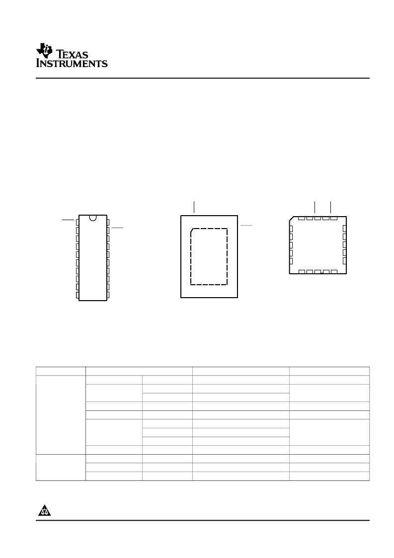
SN54LVC541A . . . J OR W PACKAGE
SN74LVC541A . . . DB, DGV, DW, NS,
OR PW PACKAGE
(TOP VIEW)
3
2
1 20 19
9 10 11 12 13
4
5
6
7
8
18
17
16
15
14
Y1
Y2
Y3
Y4
Y5
A3
A4
A5
A6
A7
SN54LVC541A . . . FK PACKAGE
(TOP VIEW)
A
A
O
Y
Y
O
A
G
Y
V
C
SN74LVC541A . . . RGY PACKAGE
(TOP VIEW)
1
20
10
11
2
3
4
5
6
7
8
9
19
18
17
16
15
14
13
12
OE2
Y1
Y2
Y3
Y4
Y5
Y6
Y7
A1
A2
A3
A4
A5
A6
A7
A8
O
Y
V
G
C
DESCRIPTION/ORDERING INFORMATION
The SN54LVC541A octal buffer/driver is designed for 2.7-V to 3.6-V V
CC
operation, and the SN74LVC541A octal
buffer/driver is designed for 1.65-V to 3.6-V V
CC
operation.
SN54LVC541A, SN74LVC541A
OCTAL BUFFERS/DRIVERS
WITH 3-STATE OUTPUTS
SCAS298M–JANUARY 1993–REVISED MAY 2005
I
off
Supports Partial-Power-Down Mode
Operation
Latch-Up Performance Exceeds 250 mA Per
JESD 17
ESD Protection Exceeds JESD 22
– 2000-V Human-Body Model (A114-A)
– 200-V Machine Model (A115-A)
– 1000-V Charged-Device Model (C101)
ABC
ORDERING INFORMATION
T
A
PACKAGE
(1)
ORDERABLE PART NUMBER
SN74LVC541ARGYR
SN74LVC541ADW
SN74LVC541ADWR
SN74LVC541ANSR
SN74LVC541ADBR
SN74LVC541APW
SN74LVC541APWR
SN74LVC541APWT
SN74LVC541ADGVR
SNJ54LVC541AJ
SNJ54LVC541AW
SNJ54LVC541AFK
TOP-SIDE MARKING
LC541A
QFN – RGY
Reel of 1000
Tube of 25
Reel of 2000
Reel of 2000
Reel of 2000
Tube of 70
Reel of 2000
Reel of 250
Reel of 2000
Tube of 20
Tube of 85
Tube of 55
SOIC – DW
LVC541A
SOP – NS
SSOP – DB
LVC541A
LC541A
–40°C to 85°C
TSSOP – PW
LC541A
TVSOP – DGV
CDIP – J
CFP – W
LCCC – FK
LC541A
SNJ54LVC541AJ
SNJ54LVC541AW
SNJ54LVC541AFK
–55°C to 125°C
(1)
Package drawings, standard packing quantities, thermal data, symbolization, and PCB design guidelines are available at
www.ti.com/sc/package.
Please be aware that an important notice concerning availability, standard warranty, and use in critical applications of Texas
Instruments semiconductor products and disclaimers thereto appears at the end of this data sheet.
PRODUCTION DATA information is current as of publication date.
Products conform to specifications per the terms of the Texas
Instruments standard warranty. Production processing does not
necessarily include testing of all parameters.
Copyright 1993–2005, Texas Instruments Incorporated
On products compliant to MIL-PRF-38535, all parameters are
tested unless otherwise noted. On all other products, production
processing does not necessarily include testing of all parameters.
相關(guān)PDF資料 |
PDF描述 |
|---|---|
| LC549 | High Power Class B Output Stage |
| LC552 | High Power Class B Amplifier |
| LC552SOIC | Analog IC |
| LC552DIP | Analog IC |
| LC561 | BLUE OVAL LAMP LED |
相關(guān)代理商/技術(shù)參數(shù) |
參數(shù)描述 |
|---|---|
| LC5442R11 | 制造商:未知廠家 制造商全稱:未知廠家 功能描述:Optoelectronic |
| LC5442R21 | 制造商:未知廠家 制造商全稱:未知廠家 功能描述:Optoelectronic |
| LC548CD | 制造商:Texas Instruments 功能描述:548CD |
| LC549 | 制造商:未知廠家 制造商全稱:未知廠家 功能描述:High Power Class B Output Stage |
| LC549MICRO | 制造商:未知廠家 制造商全稱:未知廠家 功能描述:Analog IC |
發(fā)布緊急采購,3分鐘左右您將得到回復(fù)。